NAND gate is-
a basic gate
not a universal gate
a universal gate
a universal gate
The correct Answer is:C
Step-by-Step Solution:
1. Definition of NAND Gate:
The NAND gate is a digital logic gate that outputs false only when all its inputs are true. It is the inverse of the AND gate.
2. Truth Table of NAND Gate:
The truth table for a NAND gate with two inputs (A and B) is as follows:
- When A = 0, B = 0 → Output = 1
- When A = 0, B = 1 → Output = 1
- When A = 1, B = 0 → Output = 1
- When A = 1, B = 1 → Output = 0
Thus, the output can be summarized as:
A|B|Output0|0|10|1|11|0|11|1|0
3. Why is it called a Universal Gate?:
The NAND gate is termed a universal gate because it can be used to create any other type of logic gate, including AND, OR, and NOT gates.
4. Implementation of AND Gate using NAND Gates:
- To create an AND gate using NAND gates, connect the outputs of a NAND gate back to its inputs.
- For inputs A and B, the output of the first NAND gate is \( \overline{A \cdot B} \).
- If we take this output and feed it into another NAND gate (with both inputs being the output of the first NAND gate), we get:
\(
\text{Output} = \overline{\overline{A \cdot B}} = A \cdot B
\)
Thus, we have constructed an AND gate.
5. Implementation of OR Gate using NAND Gates:
- To create an OR gate, first, invert both inputs using NAND gates.
- Connect inputs A and B to two separate NAND gates to get \( \overline{A} \) and \( \overline{B} \).
- Then, connect these outputs to another NAND gate:
\(
\text{Output} = \overline{\overline{A} \cdot \overline{B}} = A + B
\)
Thus, we have constructed an OR gate.
6. Implementation of NOT Gate using NAND Gates:
- To create a NOT gate, connect the input A to both inputs of a NAND gate:
\(
\text{Output} = \overline{A \cdot A} = \overline{A}
\)
Thus, we have constructed a NOT gate.
7. Conclusion:
Since the NAND gate can be used to construct NOT, AND, and OR gates, it is classified as a universal gate.
Final Answer:
The NAND gate is a universal gate because it can be used to implement NOT, AND, and OR gates.
---
The NAND gate is a digital logic gate that outputs false only when all its inputs are true. It is the inverse of the AND gate.
The truth table for a NAND gate with two inputs (A and B) is as follows:
- When A = 0, B = 0 → Output = 1
- When A = 0, B = 1 → Output = 1
- When A = 1, B = 0 → Output = 1
- When A = 1, B = 1 → Output = 0
Thus, the output can be summarized as:
A|B|Output0|0|10|1|11|0|11|1|0
The NAND gate is termed a universal gate because it can be used to create any other type of logic gate, including AND, OR, and NOT gates.
- To create an AND gate using NAND gates, connect the outputs of a NAND gate back to its inputs.
- For inputs A and B, the output of the first NAND gate is \( \overline{A \cdot B} \).
- If we take this output and feed it into another NAND gate (with both inputs being the output of the first NAND gate), we get:
\(
\text{Output} = \overline{\overline{A \cdot B}} = A \cdot B
\)
Thus, we have constructed an AND gate.
- To create an OR gate, first, invert both inputs using NAND gates.
- Connect inputs A and B to two separate NAND gates to get \( \overline{A} \) and \( \overline{B} \).
- Then, connect these outputs to another NAND gate:
\(
\text{Output} = \overline{\overline{A} \cdot \overline{B}} = A + B
\)
Thus, we have constructed an OR gate.
- To create a NOT gate, connect the input A to both inputs of a NAND gate:
\(
\text{Output} = \overline{A \cdot A} = \overline{A}
\)
Thus, we have constructed a NOT gate.
Since the NAND gate can be used to construct NOT, AND, and OR gates, it is classified as a universal gate.
The NAND gate is a universal gate because it can be used to implement NOT, AND, and OR gates.
Topper's Solved these Questions
- SEMICONDUCTORSBOOK - RESONANCE ENGLISHCHAPTER - SEMICONDUCTORSEXERCISE - Exercise 2
16 Videos
- SEMICONDUCTORSBOOK - RESONANCE ENGLISHCHAPTER - SEMICONDUCTORSEXERCISE - Exercise 3
88 Videos
- SEMICONDUCTORSBOOK - RESONANCE ENGLISHCHAPTER - SEMICONDUCTORSEXERCISE - Exercise 3
88 Videos
- REVISION DPPBOOK - RESONANCE ENGLISHCHAPTER - REVISION DPPEXERCISE - All Questions
463 Videos
- SIMPLE HARMONIC MOTION BOOK - RESONANCE ENGLISHCHAPTER - SIMPLE HARMONIC MOTION EXERCISE - Advanced Level Problems
13 Videos
Similar Questions
Knowledge Check
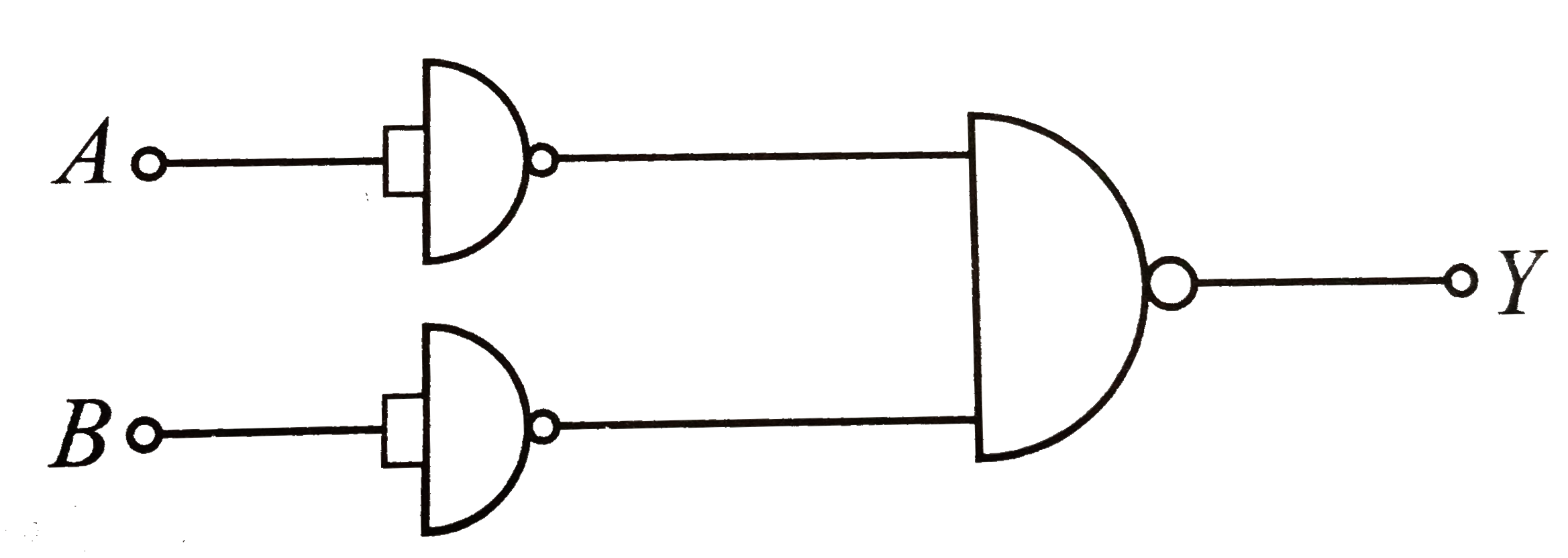
The combination of NAND gates is shown in figure.The equivalent circuit is
 AAND gateBNOR gateCOR gateDNOT gate
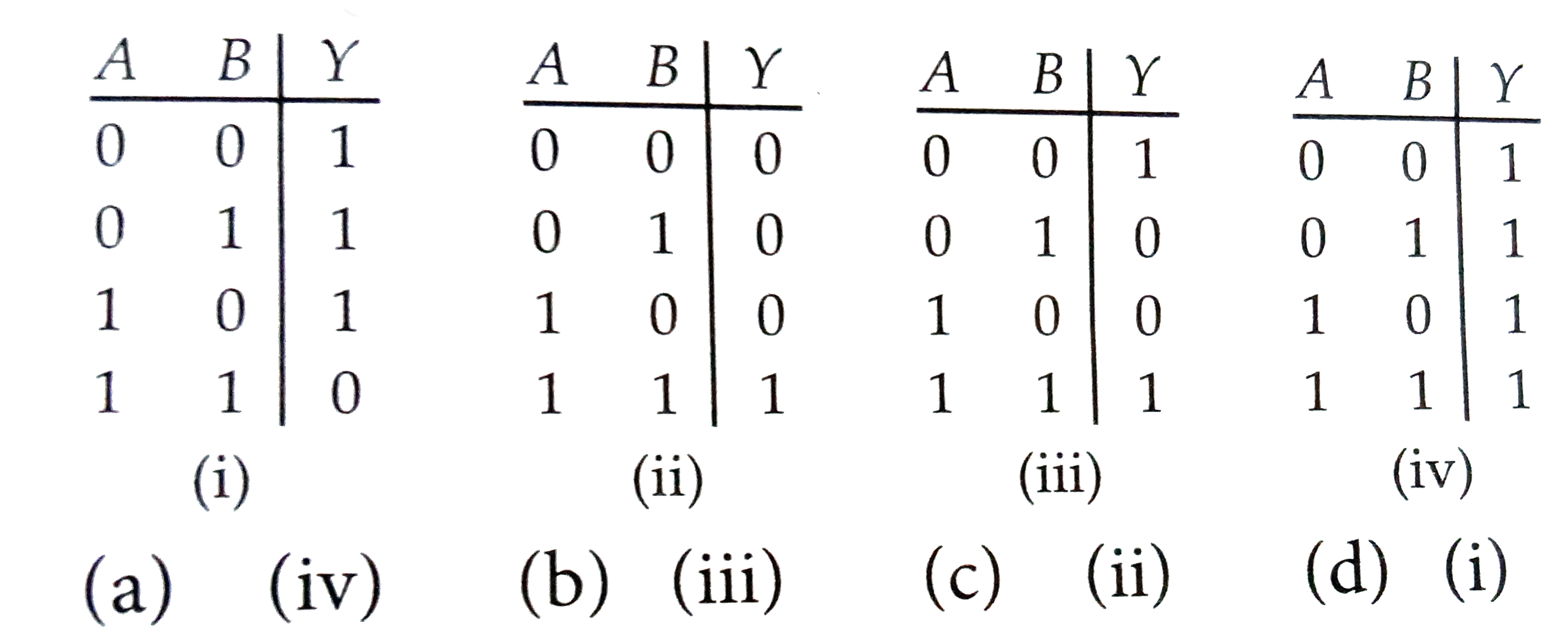
Which of the following truth tables corresponds to NAND gate ?
 A(iv)B(iii)C(ii)D(i)
Write the truth table for a NAND gate as given in Fig.9. Hence identify the exact logic operation carried out by this circuit.

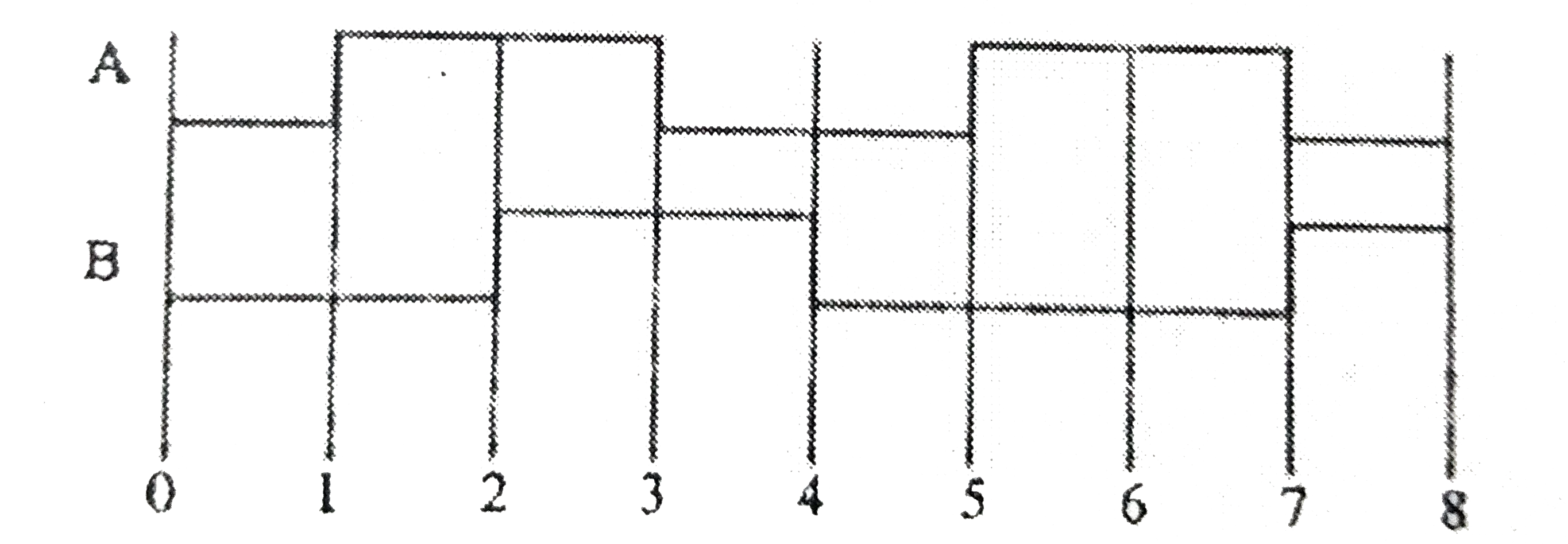
View Solution(i) Sketch the output waveform from an AND gate for the inputs A and B shown in the figure.

(ii) If the output of the above AND gate is fed to a NOT gate, name the gate of the combination so formed.
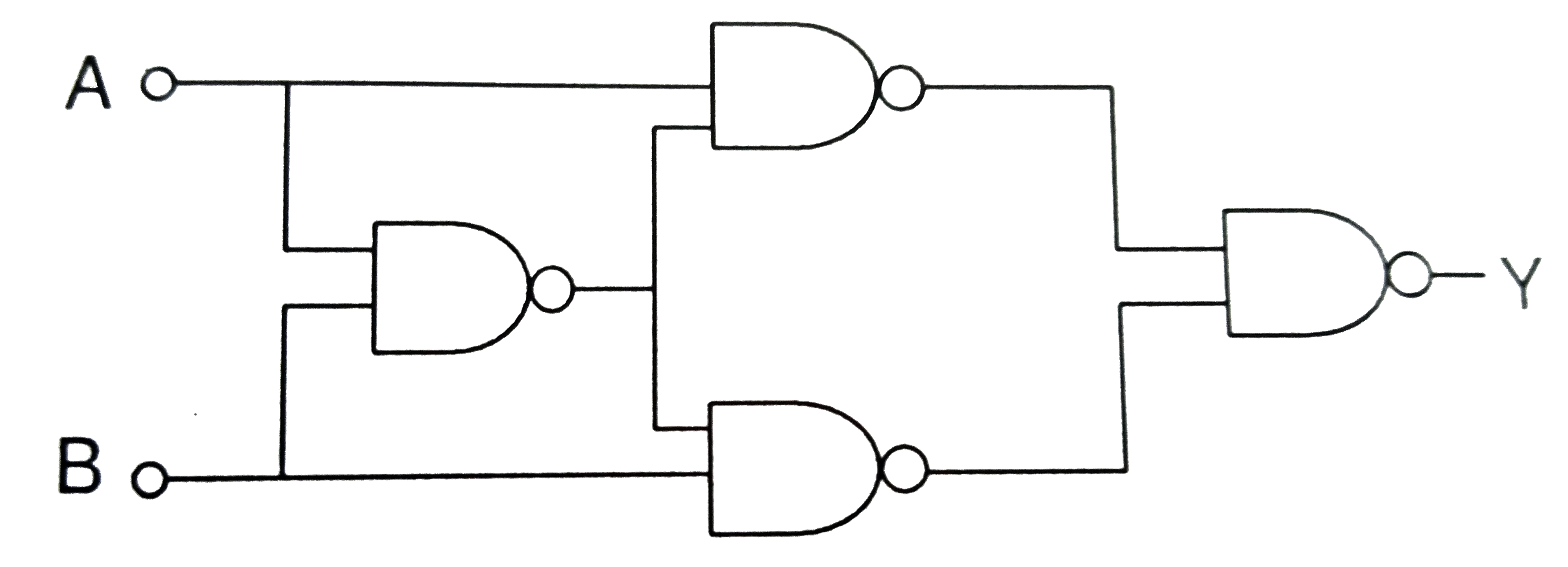
View SolutionAn AND gate is following by a NOT gate in series. With two inputs A & B, the Boolean expression for the out put Y will be :
View SolutionWhich of the following represents NAND gate ?
View SolutionGive the logic symbol of NAND gate.
View SolutionWhat is a NAND gate ? Write its truth table.
View Solution

