The given transistor operates is saturation region then what should the be value of VBB
(Rout=200Ω,Rin=100KΩ,VCC=3volt,VBE=0.7volt,VCE=0,β=200)

a. 4.1 volt
b. 7.5 volt
c. 8.2 volt
d. 6.8 volt
The correct Answer is:C
VCE=VCC−ICRO⇒0=3−IC×200
IC=3200=15mA
β=200=ICIB⇒IB=ICβ=15mA200=75μA
VBE=VBB−IBRin
VBB=0.7+75×10−6×100×103
=0.7+7.5=8.2volt
Similar Questions
In the given transistor circuit, the base current is 35μA. The value of Rα is VAB is assumed to negiligible :-
_E01_409_Q01.png)
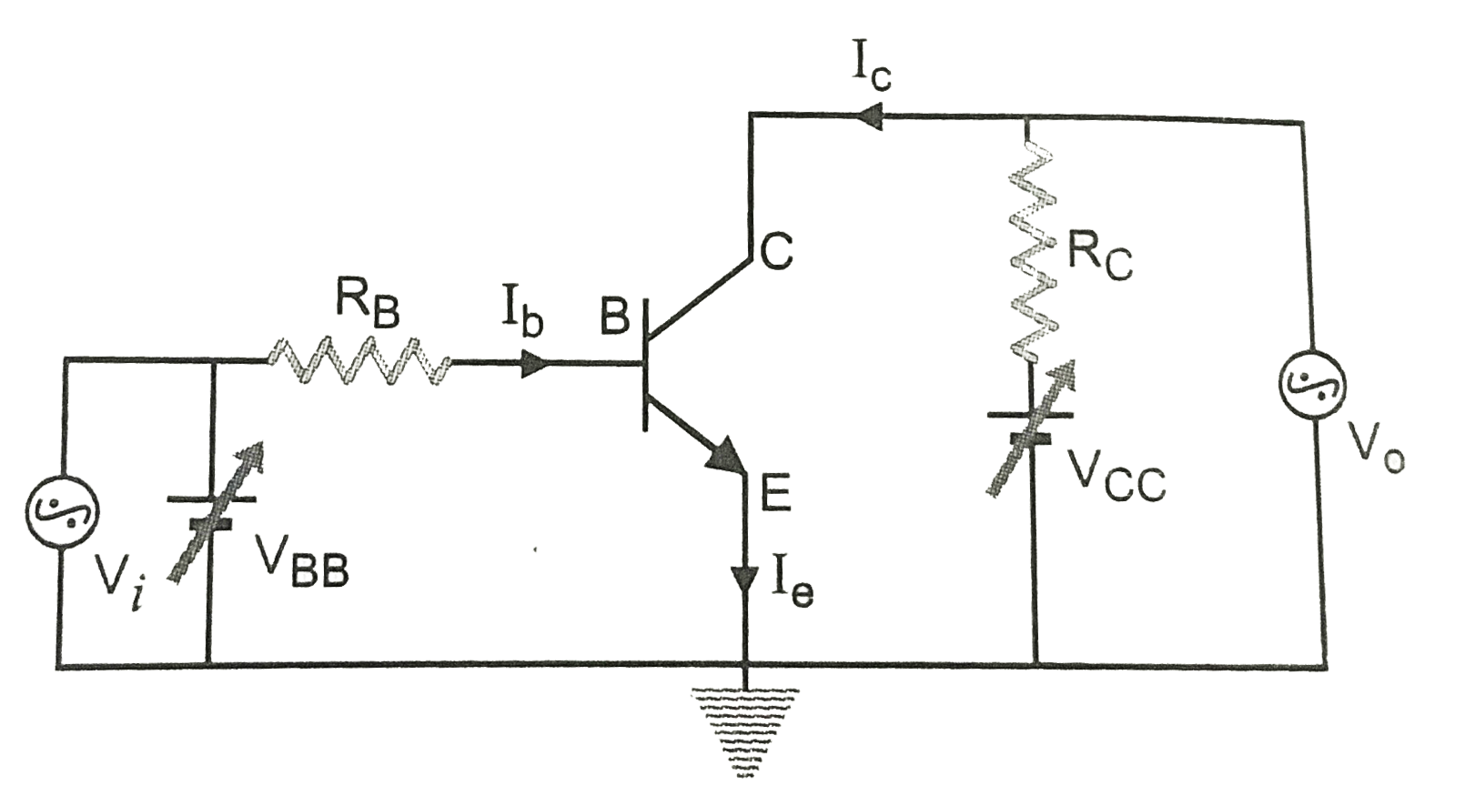
View SolutionIn common emitter transistor as shown in Fig., the VBB supply can be varied from 0 V to 5.0V. The Si. Transistor has βac=250 and RB=100kΩ,Rc=1kΩ,VCC=5.0V. Assume that when the transistor is saturated, VCE=0V and VBE=0.8V. Calculate the minimum base current, for which the transistor will reach saturation. Hence, determine Vi when the transistor is 'switched on' find ranges of Vi for which the transistor is switched off and switched on.
View Solution
Knowledge Check
In the cuircuit shown here the transistor used has a current gain β=100. What should be the bias resistor RBE so that VCE=5V(neglect VBE)
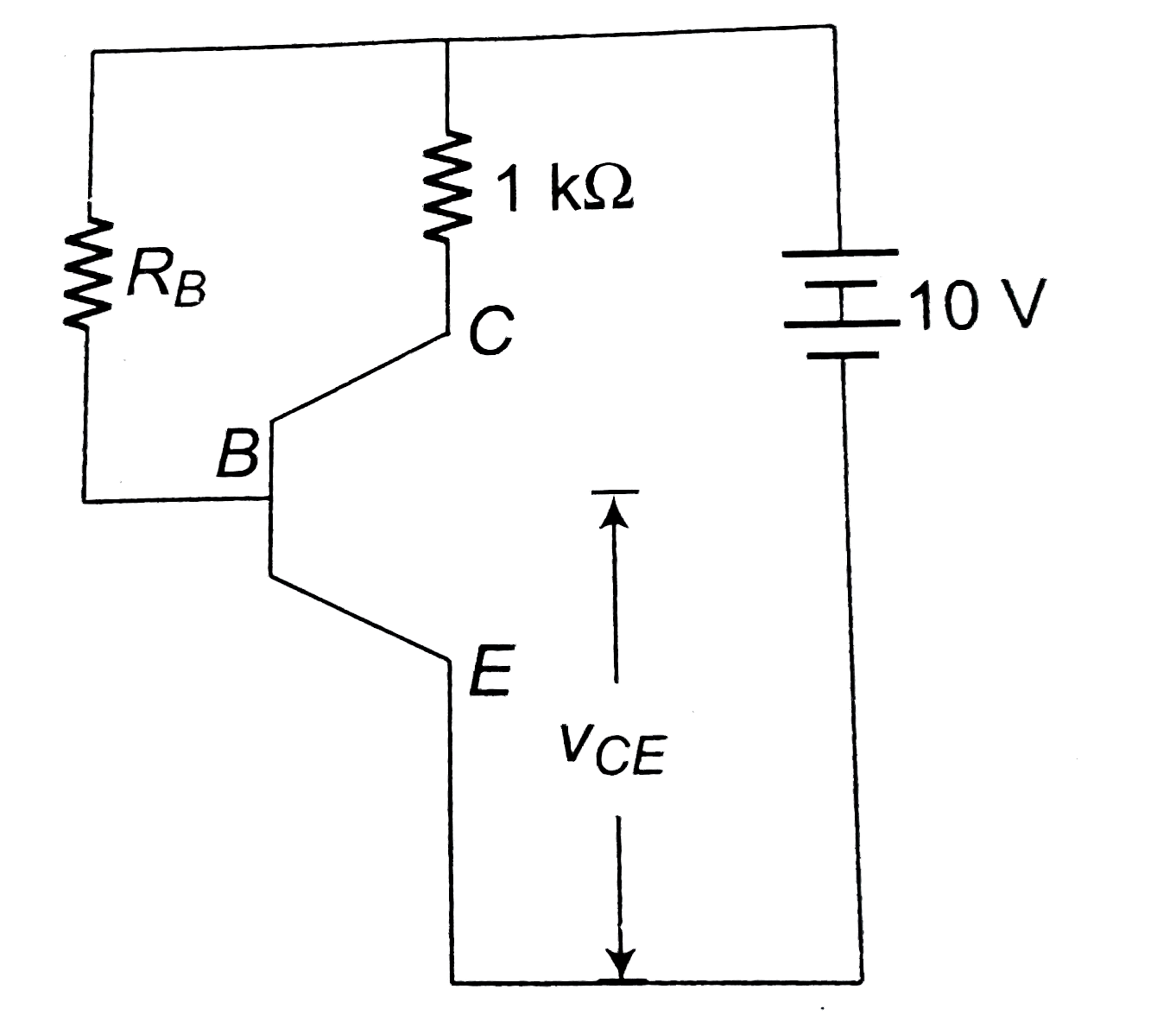 A200×103ΩB1×106ΩC500ΩD2×103Ω
A transistor connected in common emitter mode, the voltage drop across the collector is 2 V and β is 50, the base current if RC is 2kΩ is
A40μAB20μAC30μAD15μA
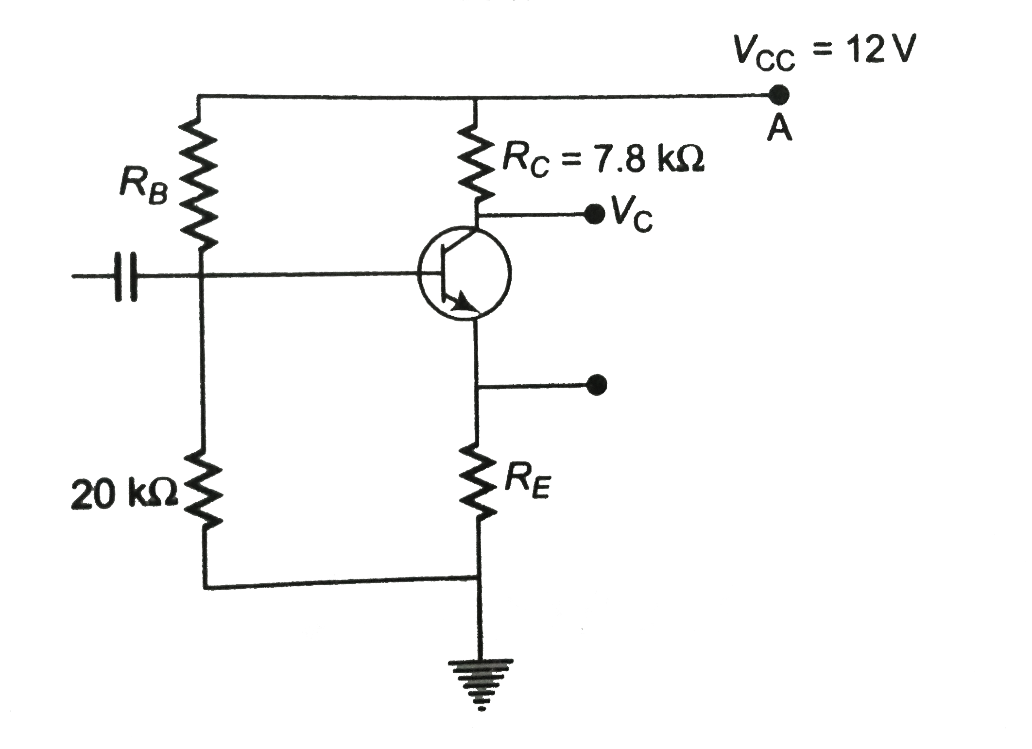
For the transistor circuit shown in figure , evaluate VE,RBandRE. Given IC=1mA,
VCE=3V,VBE=0.5V,VC=12Vandβ=100
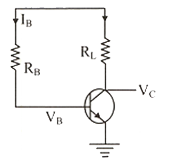
View SolutionIn the circuit of CE amplifier, a silicon transistor is used. The value of VCC=+20V,RL=3kΩ, collector voltage =5v,β=100. Then the base resistance RB should be ……×105Ω
(Take input voltage drop across Si transistor = 0.7 V)
View SolutionConsider the circuit arrangnent shown in Fig. for studying input and output characteristics of npn transistor in CE configuration.
Select the values of R and R for a transistor whose VBE=0.7V, so that the transistor is operating at point Q as shown in the characteristics shown in Fig.
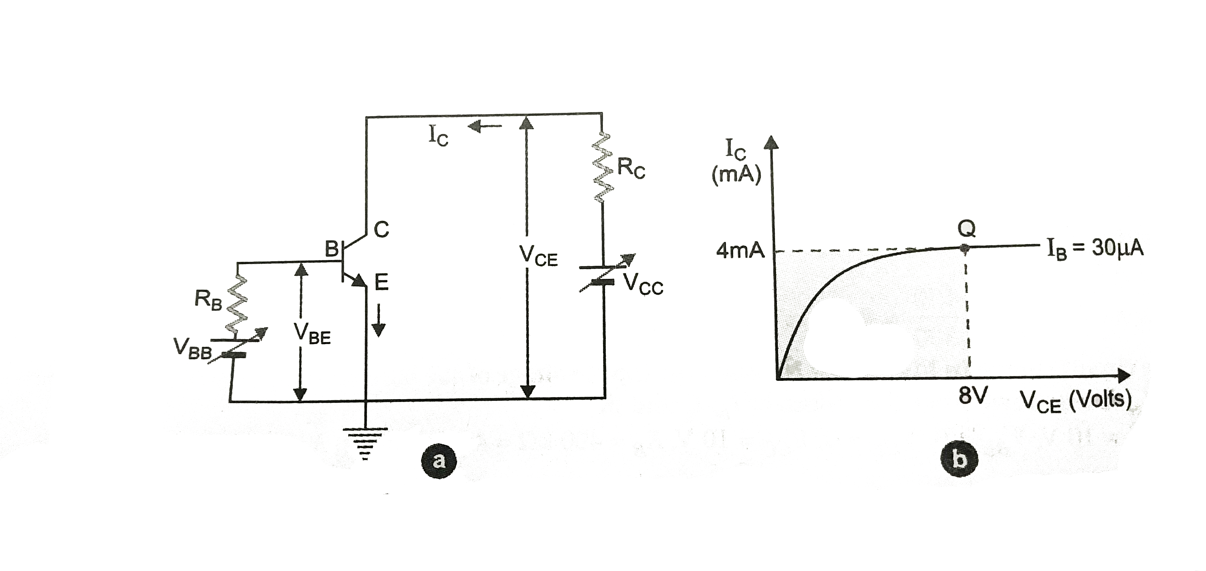 Given that the input impedance of the transistor is very small and VCC=VBB=16V, also find the voltage gain and power gain of circuit making appropriate assumptions.
View SolutionFor a common emitter transistor working in active state, following data is given RL=1KΩ Vin=10mV
△IB=15μA,△IC=3mA. The input resistance ri& voltage gain AV for the transitor is
View SolutionWhat is VA−VB in the arrangement shown in.What is the condition such that VA−VB=0
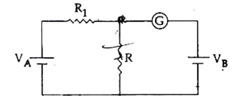
View SolutionIn the circuit shown the cells A and B have negligible resistance. For VA=12V,R1=500Ω and R=100Ω the galvanometer (G) shows no deflection. The value of VB is
View Solution