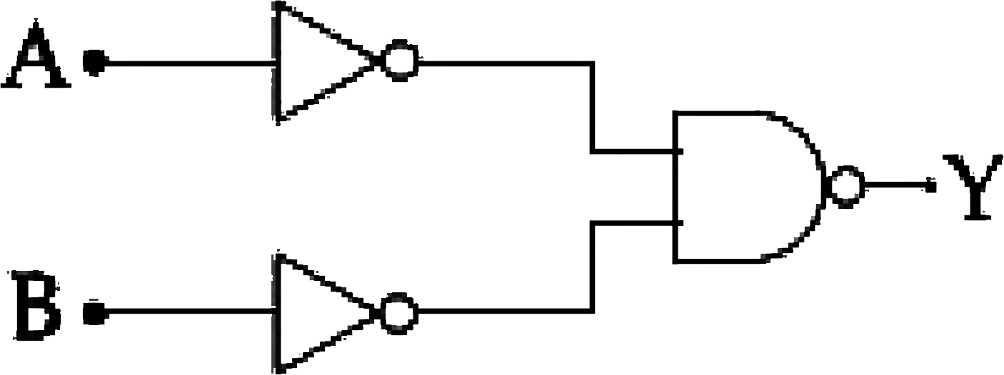
When all the inputs of a NAND gate are connected together, the resulting circuit is :-
a NOT gate
an AND gate
an OR gate
a NOR gate
The correct Answer is:A
To solve the question, we need to analyze the behavior of a NAND gate when all its inputs are connected together. Let's break it down step by step.
1. Understanding the NAND Gate:
The NAND gate is a digital logic gate that outputs false only when all its inputs are true. The logic expression for a NAND gate with two inputs A and B is given by:
Y=¯¯¯¯¯¯¯¯¯¯¯¯A⋅B
where ¯ denotes the NOT operation.
2. Connecting Inputs Together:
When all inputs of the NAND gate are connected together, let's denote this common input as A. In this case, both inputs of the NAND gate can be considered equal:
A=B=C=...=A
3. Substituting the Inputs:
Now, substituting the inputs into the NAND gate equation, we have:
Y=¯¯¯¯¯¯¯¯¯¯¯¯A⋅A
This simplifies to:
Y=¯¯¯¯¯¯A2
Since A2=A (in Boolean algebra), we can further simplify this to:
Y=¯¯¯¯A
4. Identifying the Resulting Circuit:
The expression Y=¯¯¯¯A is the characteristic equation of a NOT gate. Therefore, when all inputs of a NAND gate are connected together, the resulting circuit behaves like a NOT gate.
5. Conclusion:
Based on our analysis, the correct answer to the question is that the resulting circuit is a NOT gate.
Final Answer:
The resulting circuit is a NOT gate.
The NAND gate is a digital logic gate that outputs false only when all its inputs are true. The logic expression for a NAND gate with two inputs A and B is given by:
Y=¯¯¯¯¯¯¯¯¯¯¯¯A⋅B
where ¯ denotes the NOT operation.
When all inputs of the NAND gate are connected together, let's denote this common input as A. In this case, both inputs of the NAND gate can be considered equal:
A=B=C=...=A
Now, substituting the inputs into the NAND gate equation, we have:
Y=¯¯¯¯¯¯¯¯¯¯¯¯A⋅A
This simplifies to:
Y=¯¯¯¯¯¯A2
Since A2=A (in Boolean algebra), we can further simplify this to:
Y=¯¯¯¯A
The expression Y=¯¯¯¯A is the characteristic equation of a NOT gate. Therefore, when all inputs of a NAND gate are connected together, the resulting circuit behaves like a NOT gate.
Based on our analysis, the correct answer to the question is that the resulting circuit is a NOT gate.
The resulting circuit is a NOT gate.
Topper's Solved these Questions
- SEMICONDUCTORSBOOK - ALLENCHAPTER - SEMICONDUCTORSEXERCISE - Part-3(Exercise-2)
49 Videos
- SEMICONDUCTORSBOOK - ALLENCHAPTER - SEMICONDUCTORSEXERCISE - Part-3(Exercise-3)
27 Videos
- SEMICONDUCTORSBOOK - ALLENCHAPTER - SEMICONDUCTORSEXERCISE - Part-3(Exercise-4)
51 Videos
- PHYSICAL WORLD, UNITS AND DIMENSIONS & ERRORS IN MEASUREMENT BOOK - ALLENCHAPTER - PHYSICAL WORLD, UNITS AND DIMENSIONS & ERRORS IN MEASUREMENT EXERCISE - EXERCISE-IV
8 Videos
- WAVES AND OSCILLATIONSBOOK - ALLENCHAPTER - WAVES AND OSCILLATIONSEXERCISE - Part-1(Exercise-05)[B]
42 Videos
Similar Questions
Knowledge Check
The combination of NAND gates is shown in figure.The equivalent circuit is
 AAND gateBNOR gateCOR gateDNOT gate
The real time variation of input signals A and B are as shown below. If the inputs are fed into NAND gate, then select the output signal from the following :-
_E01_434_Q01.png) A
A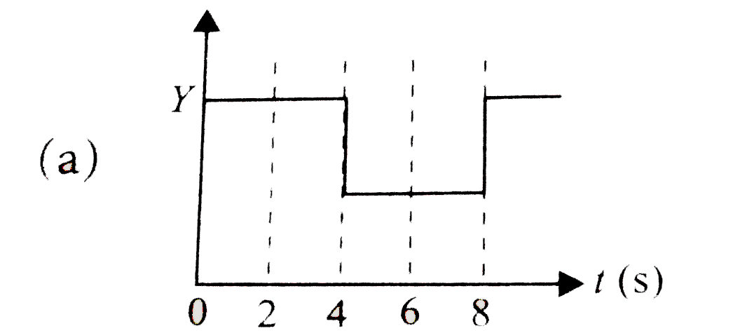 B
B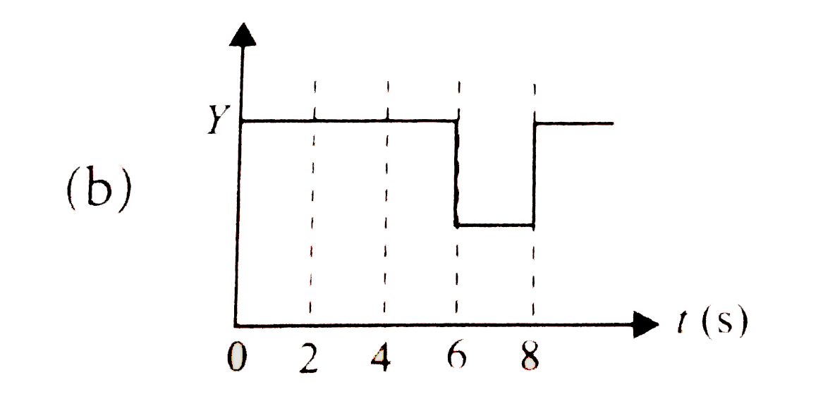 C
C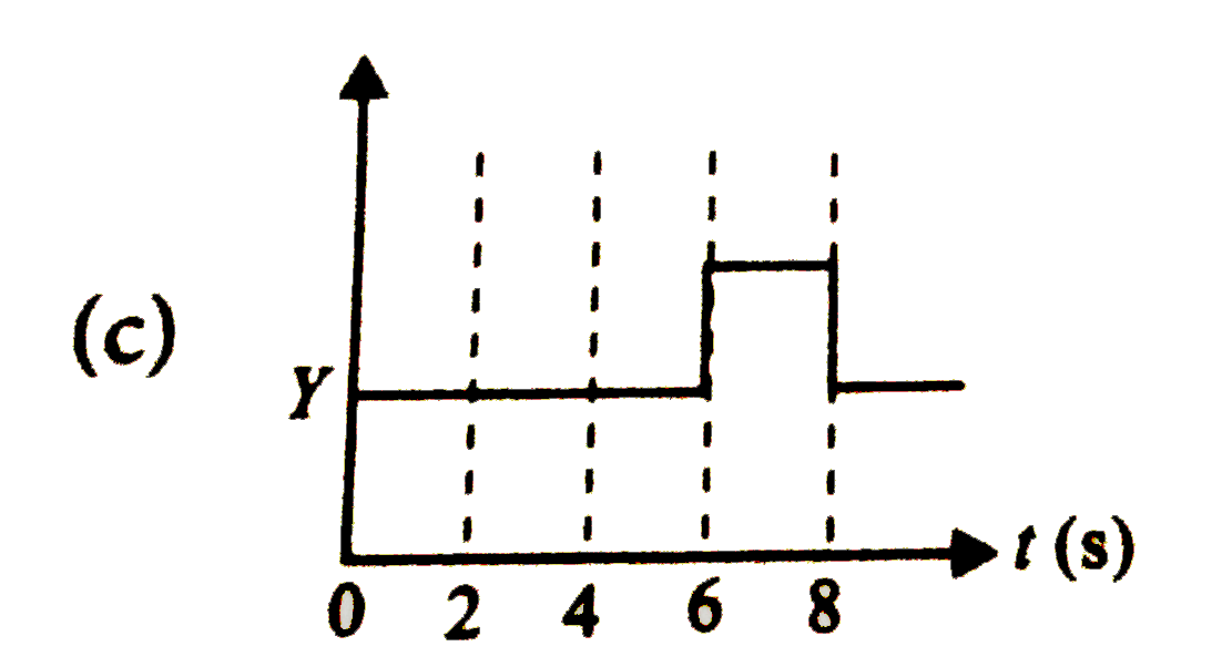 D
D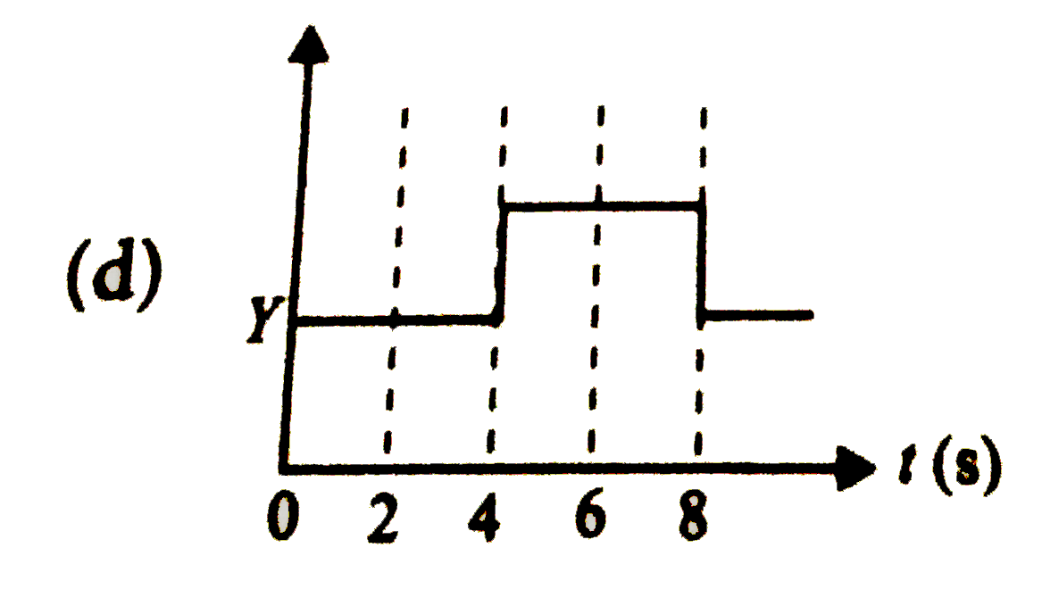
The resultant resistance value of n resistance each of r ohms and connected is series is X. When those n , resistance are connected in parallel , the resultant values is .
View SolutionGive the logic symbol of NAND gate.
View SolutionWhat is a NAND gate ? Write its truth table.
View SolutionWhen the inputs of a two input logic gate are 0 and 0, the output is 1. When the inputs are 1 and 0, the output is zero. The type of logic gate is
View SolutionThe output of an OR gate is connected to both the inputs of a NAND gate. The combination will serve as a
View SolutionWhich of the following represents NAND gate ?
View Solution

