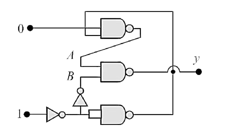
In the circuit shown in the following figure, the value of Y is
A
0
B
1
C
fluctuates between O and 1
D
indeterminate as the circuit cannot be realized
Video Solution
Text Solution
The correct Answer is:A
Lower NOT gate inverts input to zero. NOT gate from NAND gate inverts this output to 1 and upper NAND gate converts this input 1 and input Oto 1.
Thus A = 1 and B = 1 become inputs of NAND gate giving final output as zero. Choice A is correct.
|
Topper's Solved these Questions
Similar Questions
Knowledge Check
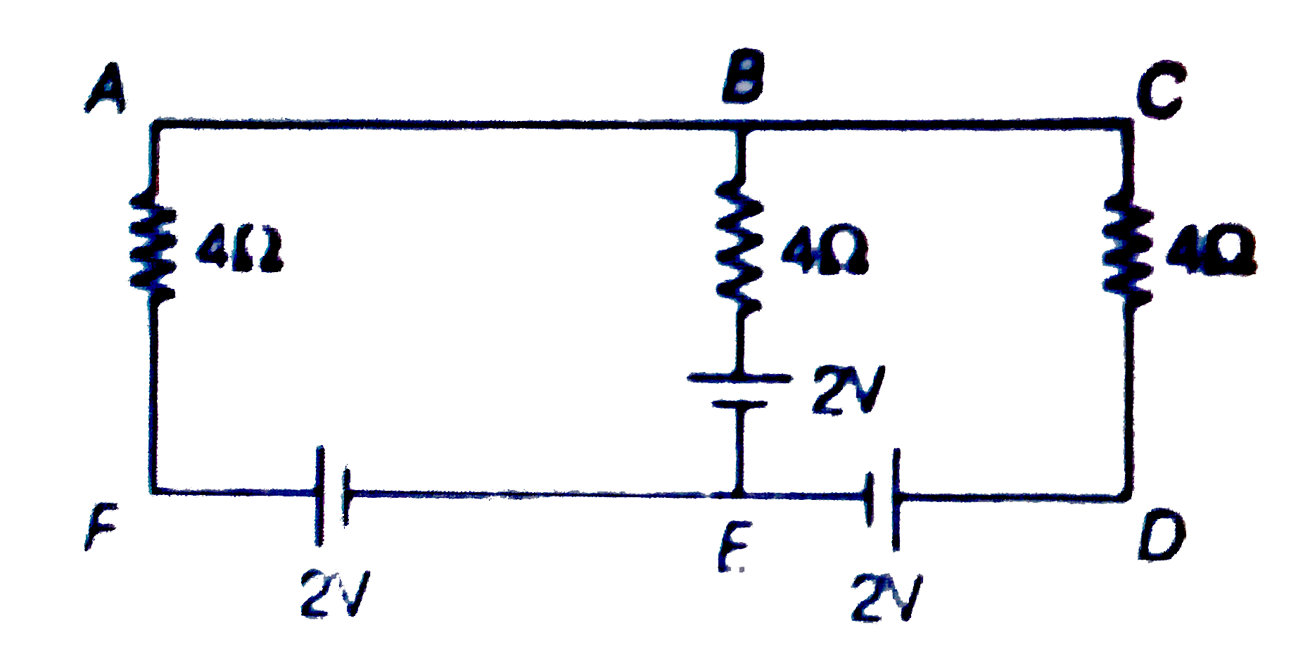
For the circuit shown in the following figure, the
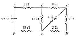 APotential difference between points B and E is 5 VBPotential difference between points A and B is 10 VCCurrent in the 4Ω resistor is 0.25ADCurrent in the 4Ω resistor is 0.5 A
For the circuit shown in the following figure,
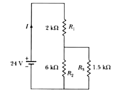 AThe current I through the battery is 7.5 mABThe potential difference across R3 is 18 VCRatio of powers dissipated in R1andR2 is 3DIf R1andR2 are interchanged, magnitude of the power dissipated in R3 will decrease by a factor of 9
For the circuit shown in the following figure.
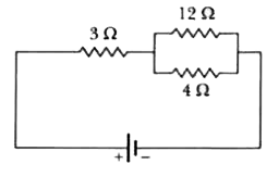 AThe heat dissipated in 4Ω resistance is more than that dissipated in 12Ω resistanceBMaximum heat is dissipated in 3Ω resistanceCThe heat dissipated in 12Ω resistance is more than that dissipated in 4Ω resistanceDThe power dissipated in 3Ω resistance is 18 W

