Which type of biasing gives a semi-conductor diode very high resistance?
To determine which type of biasing gives a semiconductor diode very high resistance, we can analyze the two types of biasing: forward biasing and reverse biasing.
1. Understanding Diode Biasing:
- A semiconductor diode has two terminals: the p-side (positive) and the n-side (negative).
- There are two types of biasing: forward biasing and reverse biasing.
2. Forward Biasing:
- In forward biasing, the positive terminal of the battery is connected to the p-side of the diode, and the negative terminal is connected to the n-side.
- This configuration allows current to flow through the diode easily because the applied voltage reduces the potential barrier at the junction.
3. Effect of Forward Biasing:
- When forward biasing occurs, the electric field at the junction is reduced due to the opposing electric field created by the applied voltage.
- As a result, the resistance of the diode in forward bias is low, allowing significant current to flow.
4. Reverse Biasing:
- In reverse biasing, the positive terminal of the battery is connected to the n-side, and the negative terminal is connected to the p-side.
- This configuration increases the potential barrier at the junction, preventing current from flowing.
5. Effect of Reverse Biasing:
- In reverse biasing, the electric field at the junction is strengthened because the applied voltage adds to the existing electric field created by the depletion region.
- This results in a very high resistance at the junction, effectively blocking current flow.
6. Conclusion:
- Therefore, the type of biasing that gives a semiconductor diode very high resistance is reverse biasing.
Final Answer:
Reverse biasing gives a semiconductor diode very high resistance.
- A semiconductor diode has two terminals: the p-side (positive) and the n-side (negative).
- There are two types of biasing: forward biasing and reverse biasing.
- In forward biasing, the positive terminal of the battery is connected to the p-side of the diode, and the negative terminal is connected to the n-side.
- This configuration allows current to flow through the diode easily because the applied voltage reduces the potential barrier at the junction.
- When forward biasing occurs, the electric field at the junction is reduced due to the opposing electric field created by the applied voltage.
- As a result, the resistance of the diode in forward bias is low, allowing significant current to flow.
- In reverse biasing, the positive terminal of the battery is connected to the n-side, and the negative terminal is connected to the p-side.
- This configuration increases the potential barrier at the junction, preventing current from flowing.
- In reverse biasing, the electric field at the junction is strengthened because the applied voltage adds to the existing electric field created by the depletion region.
- This results in a very high resistance at the junction, effectively blocking current flow.
- Therefore, the type of biasing that gives a semiconductor diode very high resistance is reverse biasing.
Reverse biasing gives a semiconductor diode very high resistance.
Topper's Solved these Questions
- BOOK - AAKASH SERIESCHAPTER - SEMICONDUCTOR DEVICESEXERCISE - Problems (LEVEL-I)35videos
SEMICONDUCTOR DEVICES
- BOOK - AAKASH SERIESCHAPTER - SEMICONDUCTOR DEVICESEXERCISE - Problems (LEVEL-II)9videos
SEMICONDUCTOR DEVICES
- BOOK - AAKASH SERIESCHAPTER - SEMICONDUCTOR DEVICESEXERCISE - Exercise (Short answer questions)27videos
SEMICONDUCTOR DEVICES
- BOOK - AAKASH SERIESCHAPTER - RAY OPTICSEXERCISE - PROBLEMS ( LEVEL-II)60videos
RAY OPTICS
- BOOK - AAKASH SERIESCHAPTER - UNITS AND MEASUREMENTEXERCISE - PRACTICE EXERCISE45videos
UNITS AND MEASUREMENT
Similar Questions
An n-type semi- conductor is
View SolutionAvalanche breakdown in a semi conductor diode occurs when
View SolutionTwo conducting spheres of radii r and 3r initially have charges 3q & q respectively. Their separation is much larger their radii. If they are joined by a conductor of high resistance, the force between them will :
View SolutionAssertion: In reverse biased condition a p-n junction diode does not conduct.
Reason: In reverse biased condition a diode has zero resistance.View SolutionWhat type of semi-conductors is produced when silicon is doped with arsenic?
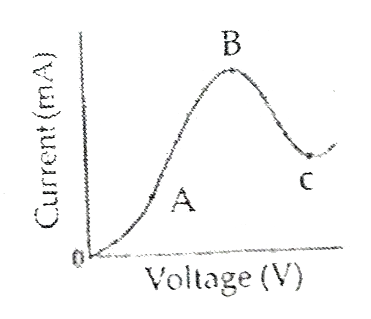
View SolutionThe graph shown in the figure represents a plot of current versus voltage for a given semi-conductor. Identify the region, if any, over which the semicondutor has a negative resistance.
 View Solution
Two identical cells of emf 1.5 V each joined in paralllel provide supply to an external circuit consisting of two resistances of 7Ω each joined in parallel. A very high resistance voltmeter reads the terminal voltage of cells to be 1.4 V. Calculate the internal resistance of each cell.
View SolutionWith reference to a semi-conductor diode, what is meant by : (i) Forward bias
(ii) Reverse bias
(iii) Depletion region.
(b) An EM wave, Y1, has a wavelength of 1 cm while another EM wave, Y2, has a frequency of 1015 Hz. Name two type of waves and write one application for each.View SolutionWith reference to a semi-conductor diode, what is meant by:
Reverse biasView SolutionWhat happens to the resistivity of semi-conductors with the increase in temperature?
View Solution

