The potential barrier at a P-n junction is due to the charges on either side of the junction. These charges are
Fixed ions
Majority carriers
Both majority and minority carriers
Minority carriers
The correct Answer is:A
To solve the question regarding the potential barrier at a P-N junction and the charges responsible for it, we can break down the explanation into clear steps:
1. Understanding P-N Junction:
- A P-N junction is formed by joining P-type and N-type semiconductors. P-type semiconductors have an abundance of holes (positive charge carriers), while N-type semiconductors have an abundance of electrons (negative charge carriers).
Hint: Remember that P-type has holes as majority carriers, and N-type has electrons.
2. Formation of the Depletion Layer:
- When the P-N junction is formed, electrons from the N-type region move towards the P-type region and recombine with holes. This movement creates a region around the junction where there are no free charge carriers, known as the depletion layer.
Hint: Focus on the movement of charge carriers across the junction and the resulting depletion layer.
3. Charge Imbalance:
- As electrons leave the N-type region, it becomes positively charged due to the fixed positive ions (donor atoms). Conversely, as holes are filled by electrons from the P-type side, it becomes negatively charged due to the fixed negative ions (acceptor atoms).
Hint: Consider the charges left behind after the recombination of carriers.
4. Potential Barrier Creation:
- The fixed positive and negative charges on either side of the depletion layer create an electric field. This electric field establishes a potential barrier that opposes further movement of charge carriers across the junction.
Hint: Think about how the electric field affects the movement of charge carriers.
5. Identifying the Charges:
- The charges responsible for the potential barrier are the fixed ions (positive and negative) that remain after the majority carriers (electrons and holes) have recombined. Therefore, the potential barrier is primarily due to the fixed charges (ions) present in the depletion region.
Hint: Remember that the potential barrier is not due to the majority or minority carriers but rather the fixed charges.
Conclusion:
The potential barrier at a P-N junction is due to the fixed ions on either side of the junction, which are created by the movement and recombination of majority carriers (electrons and holes).
Final Answer:
The charges responsible for the potential barrier at a P-N junction are fixed ions.
- A P-N junction is formed by joining P-type and N-type semiconductors. P-type semiconductors have an abundance of holes (positive charge carriers), while N-type semiconductors have an abundance of electrons (negative charge carriers).
- When the P-N junction is formed, electrons from the N-type region move towards the P-type region and recombine with holes. This movement creates a region around the junction where there are no free charge carriers, known as the depletion layer.
- As electrons leave the N-type region, it becomes positively charged due to the fixed positive ions (donor atoms). Conversely, as holes are filled by electrons from the P-type side, it becomes negatively charged due to the fixed negative ions (acceptor atoms).
- The fixed positive and negative charges on either side of the depletion layer create an electric field. This electric field establishes a potential barrier that opposes further movement of charge carriers across the junction.
- The charges responsible for the potential barrier are the fixed ions (positive and negative) that remain after the majority carriers (electrons and holes) have recombined. Therefore, the potential barrier is primarily due to the fixed charges (ions) present in the depletion region.
The potential barrier at a P-N junction is due to the fixed ions on either side of the junction, which are created by the movement and recombination of majority carriers (electrons and holes).
The charges responsible for the potential barrier at a P-N junction are fixed ions.
Topper's Solved these Questions
- SEMICONDUCTOR DEVICESBOOK - AAKASH SERIESCHAPTER - SEMICONDUCTOR DEVICESEXERCISE - EXERCISE -I (TRANSISTORS)
22 Videos
- SEMICONDUCTOR DEVICESBOOK - AAKASH SERIESCHAPTER - SEMICONDUCTOR DEVICESEXERCISE - EXERCISE -I (LOGIC GATES)
17 Videos
- SEMICONDUCTOR DEVICESBOOK - AAKASH SERIESCHAPTER - SEMICONDUCTOR DEVICESEXERCISE - EXERCISE -I (ENERGY BANDS AND CLASSIFICATION OF SOLIDS )
41 Videos
- RAY OPTICSBOOK - AAKASH SERIESCHAPTER - RAY OPTICSEXERCISE - PROBLEMS ( LEVEL-II)
60 Videos
- UNITS AND MEASUREMENTBOOK - AAKASH SERIESCHAPTER - UNITS AND MEASUREMENTEXERCISE - PRACTICE EXERCISE
45 Videos
Similar Questions
Knowledge Check
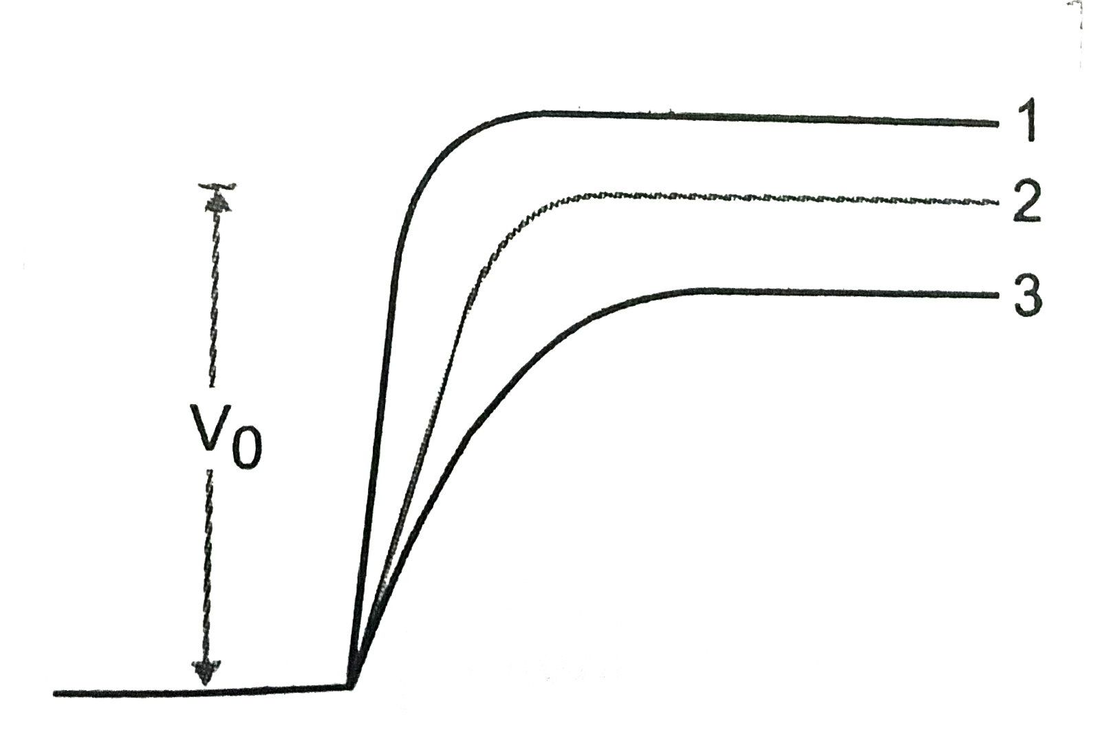
In Fig . V0 is the potential barrier across a p-n junction, when no battery is connected across the junction
 A1 and 3 both correspond to forward bias of junctionB3 corresponds to forward bias of junction and 1 corresponds to reverse bias of junctionC1 corresponds to forward bias and 3 corresponds to reverse bias of junction.D3 and 1 both correspond to reverse bias of junction.
The diffusion current in a p-n junction is
View SolutionIn junction diode, the holes are due to
View SolutionThe barrier potential in a P-N junction is maximum in
View SolutionIn Fig . V0 is the potential barrier across a p-n junction, when no battery is connected across the junction

View SolutionBarrier potential of a p−n junction diode does not depend on
View SolutionBarrier potential of a p−n junction diode does not depend on
View SolutionCan the potential barrier across a p-n junction be measured by simply connecting a voltmeter across the junction ?
View Solution
