Transfer characteristic [output voltage (V0) vs input voltage (Vi) for a base biased transistor in CE configuration is as shown in the figure. For using transistor as a switch, it is used
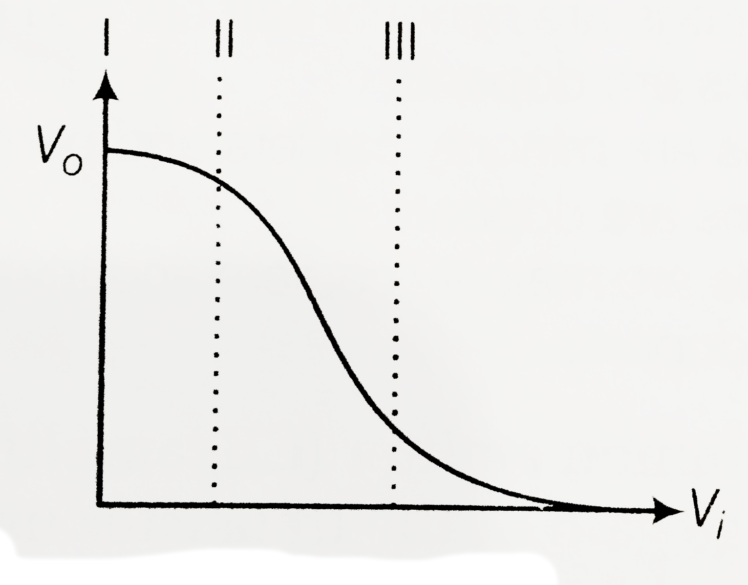
in region II
in region I
in region III
both in region (I) and (III)
The correct Answer is:D
Step by step video & image solution for Transfer characteristic [output voltage (V_(0)) vs input voltage (V_(i)) for a base biased transistor in CE configuration is as shown in the figure. For using transistor as a switch, it is used by Physics experts to help you in doubts & scoring excellent marks in Class 12 exams.
Topper's Solved these Questions
- BOOK - AAKASH SERIESCHAPTER - SEMICONDUCTOR DEVICESEXERCISE - EXERCISE -I (LOGIC GATES)17videos
SEMICONDUCTOR DEVICES
- BOOK - AAKASH SERIESCHAPTER - SEMICONDUCTOR DEVICESEXERCISE - EXERCISE -I (MATCHING TYPE QUESTIONS)9videos
SEMICONDUCTOR DEVICES
- BOOK - AAKASH SERIESCHAPTER - SEMICONDUCTOR DEVICESEXERCISE - EXERCISE -I (P-N JUNCTION DIODE)30videos
SEMICONDUCTOR DEVICES
- BOOK - AAKASH SERIESCHAPTER - RAY OPTICSEXERCISE - PROBLEMS ( LEVEL-II)60videos
RAY OPTICS
- BOOK - AAKASH SERIESCHAPTER - UNITS AND MEASUREMENTEXERCISE - PRACTICE EXERCISE45videos
UNITS AND MEASUREMENT
Similar Questions
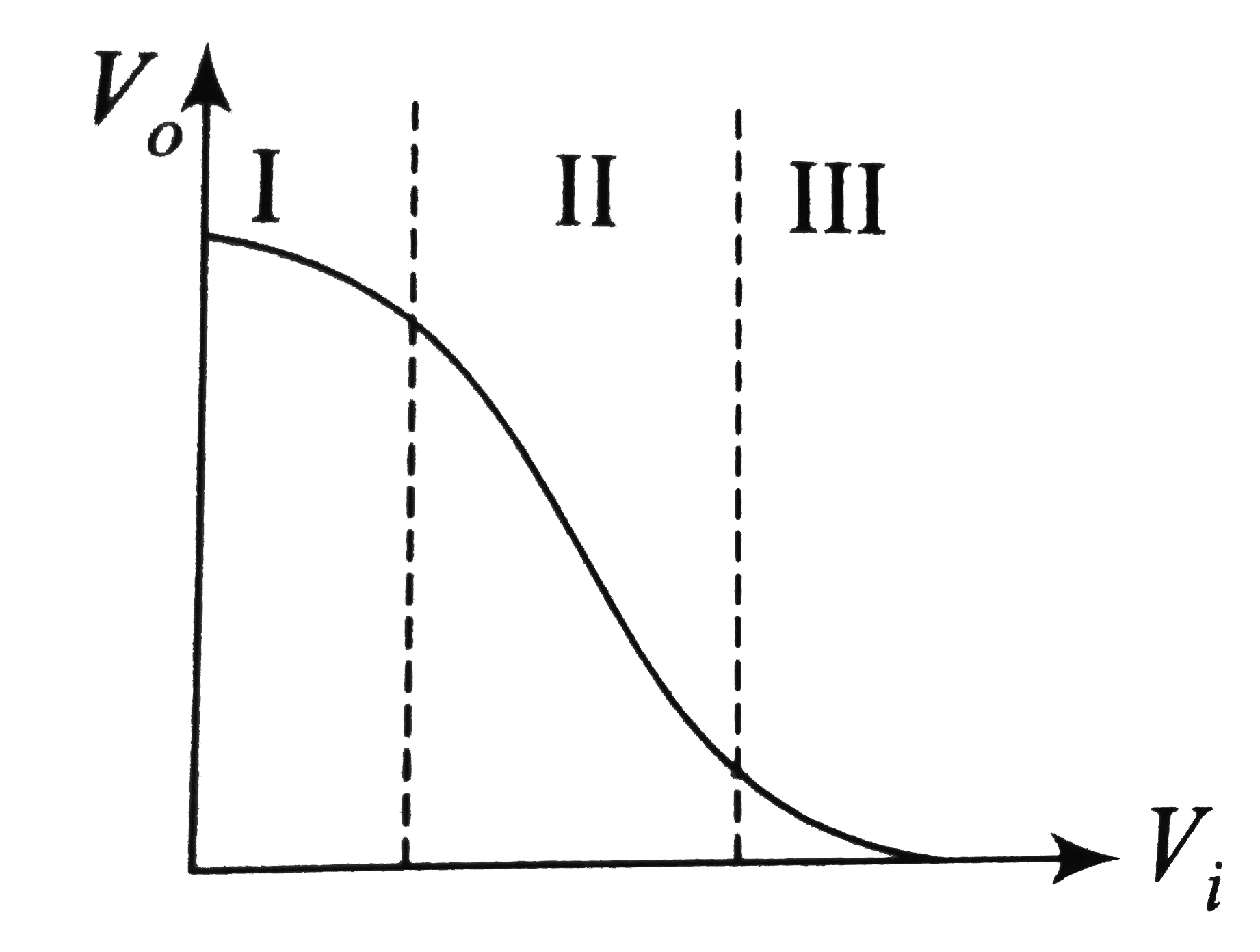
Transfer characterstics [output voltage (Vo) vs. input voltage (Vi)] for a base biased transistor in CE configuration is as shown in the figure. For using transfor as a which, it is used
 View Solution
Draw the tramsfer characteristic curve of a base biased transistor in CE configuration. Explain clearly how the active region of the Vo versus Vi curve in a transistor is used as an amplifier.
View Solution
Knowledge Check
- Question 1 - Select One
The transfer characteristics of a base biased transistor has the operation regions, namely, cutoff, active region and saturation region. For using the transistor as an amplifier it has to operate in the
Aactive regionBcutoff regionCsaturation regionDcutoff and saturation - Question 2 - Select One
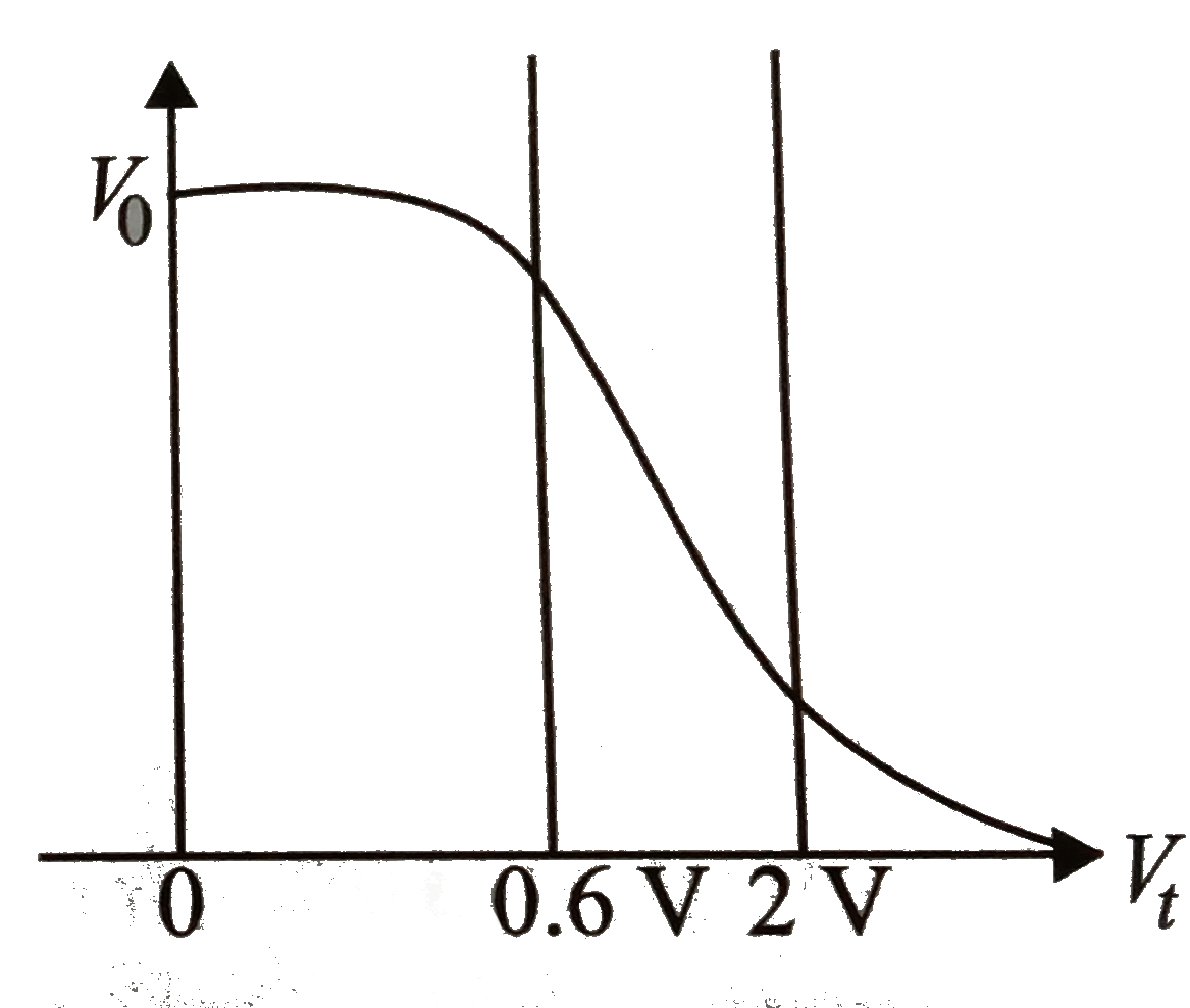
Fig.shows that transfer characteristics of a base biased CE transistor. Which of the following statements are true?
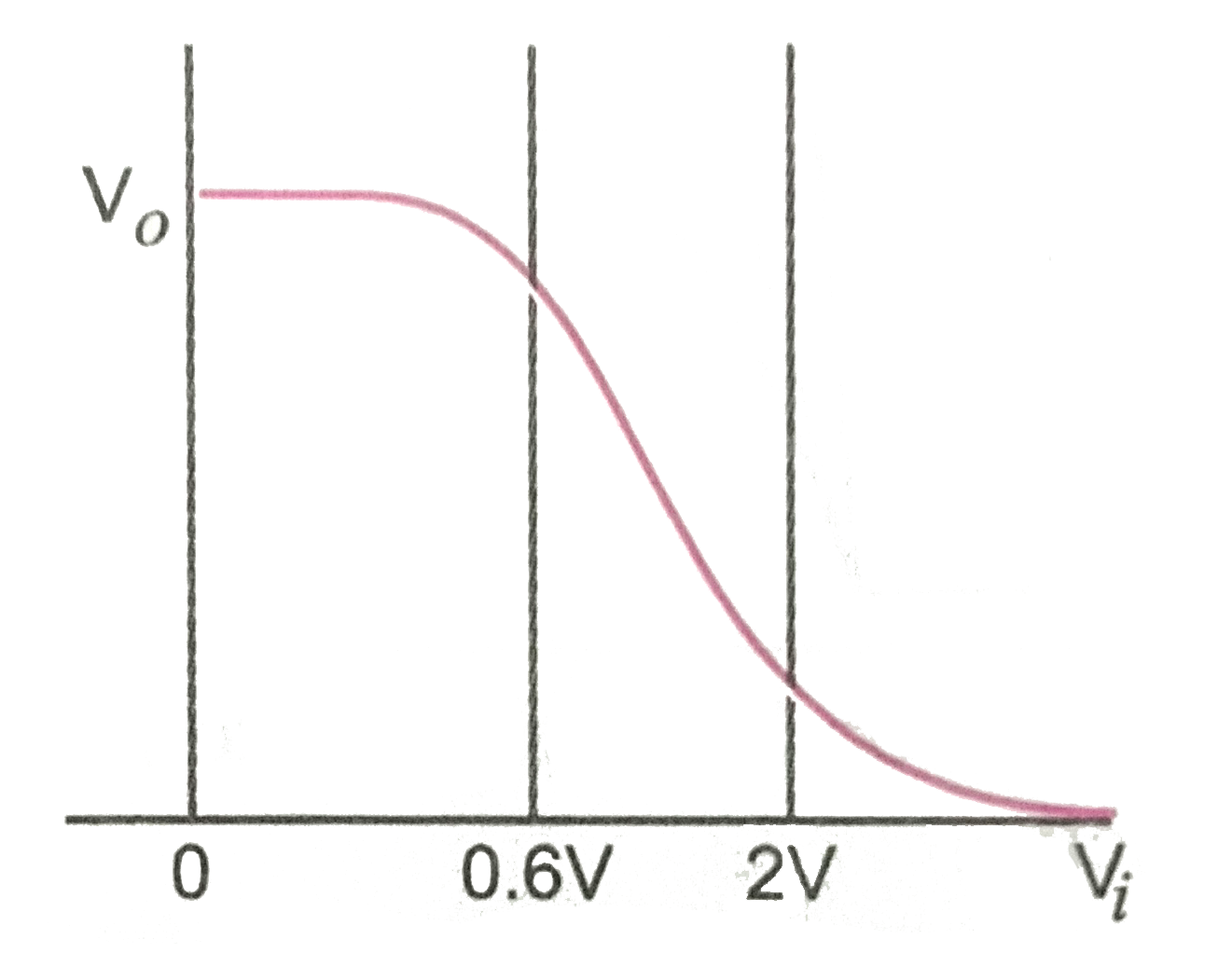 AAt Vi=1V, it can be used as an amplifierBAt Vi=0.5V, it can be used as a switch turned offCAt Vi=2.5V, it can be used as a switch turned onDAll of these
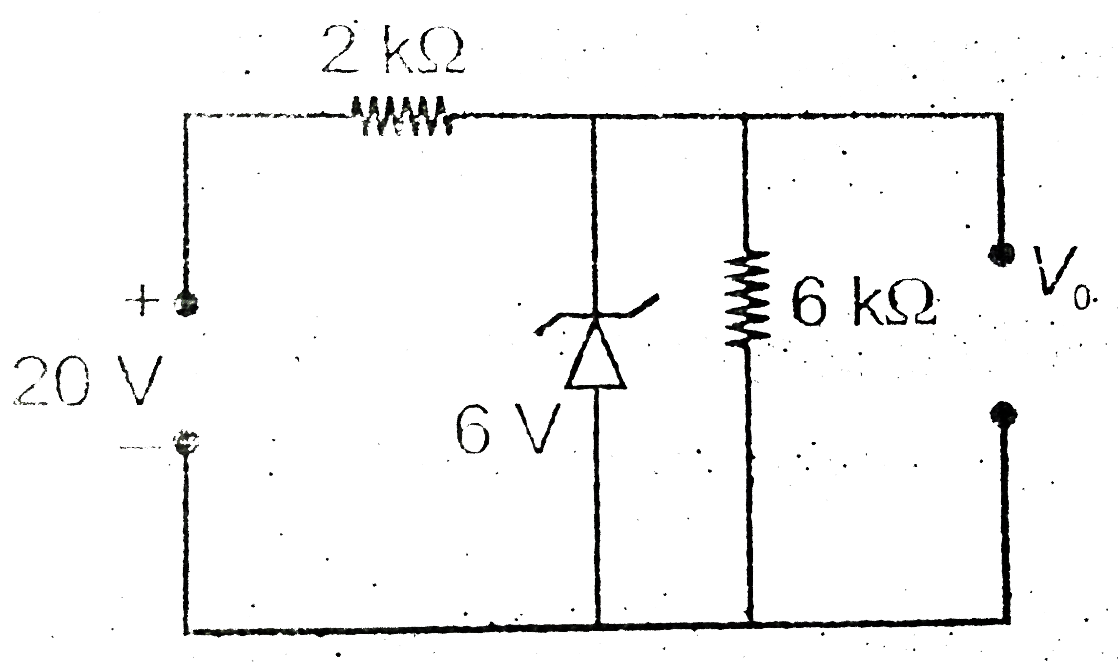
What is the value of output voltage V0 in the circuit shown in the figure ?
 View Solution
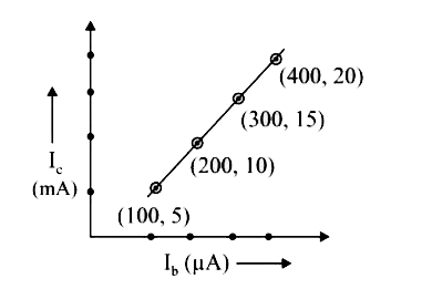
The transfer characteristic curve of a transistor, having input and output resistance 100Ωand100kΩ respectively, is shown in the figure. The Voltage and Power gain, are respectively:
 View Solution
The transfer characteristic curve of a transistor, having input and output resistance 100Ωand100kΩ respectively, is shown in the figure. The Voltage and Power gain, are respectively:
 View Solution
Output characteristics of an n-p-n transistor in CE configuration is shown in the Fig. Determine
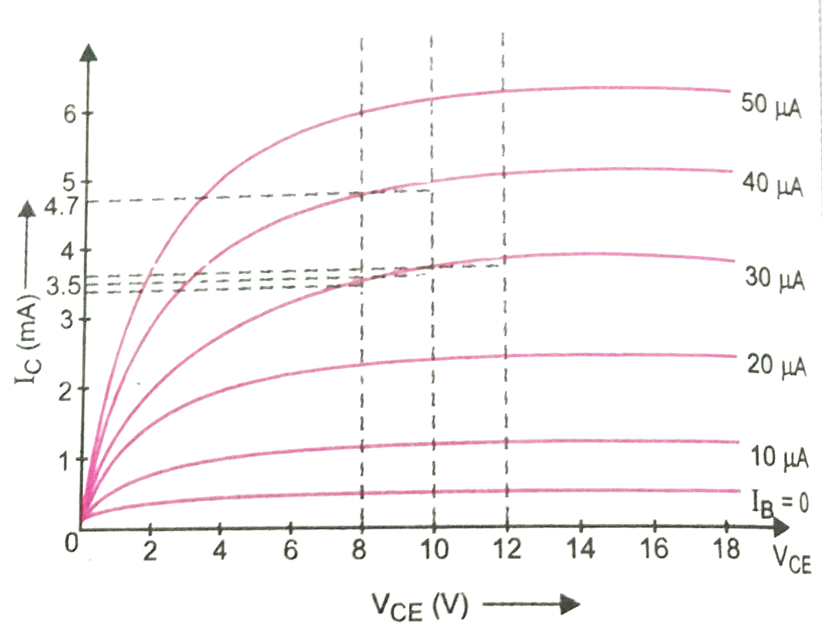
(i) dynamic output resistance (ii) dc current gain and (iii) ac current gain at an opererating point VCE=10V, when IB=30μA.View SolutionAssertion (A):∧m(H⊕) and ∧m(cOH) ions are very much higher than those of other ions.
Reason (R):It is due to proton jump from one water molecule to another resulting in a more rapid transfer of positive charge form one region to another.
(a)If both (A) and (R) are correct, and (R) is the correct explanation of (A).
(b)If both (A) and (R) are correct, but (R) is not the correct explanation of (A).
(c)If (A) is correct, but (R) is incorrect.
(d)If (A) is incorrect, (R) is correct.View SolutionThe transfer characteristics of a base biased common emitter transistor is shown in the figure. Which of the following statements are true?
 View Solution

