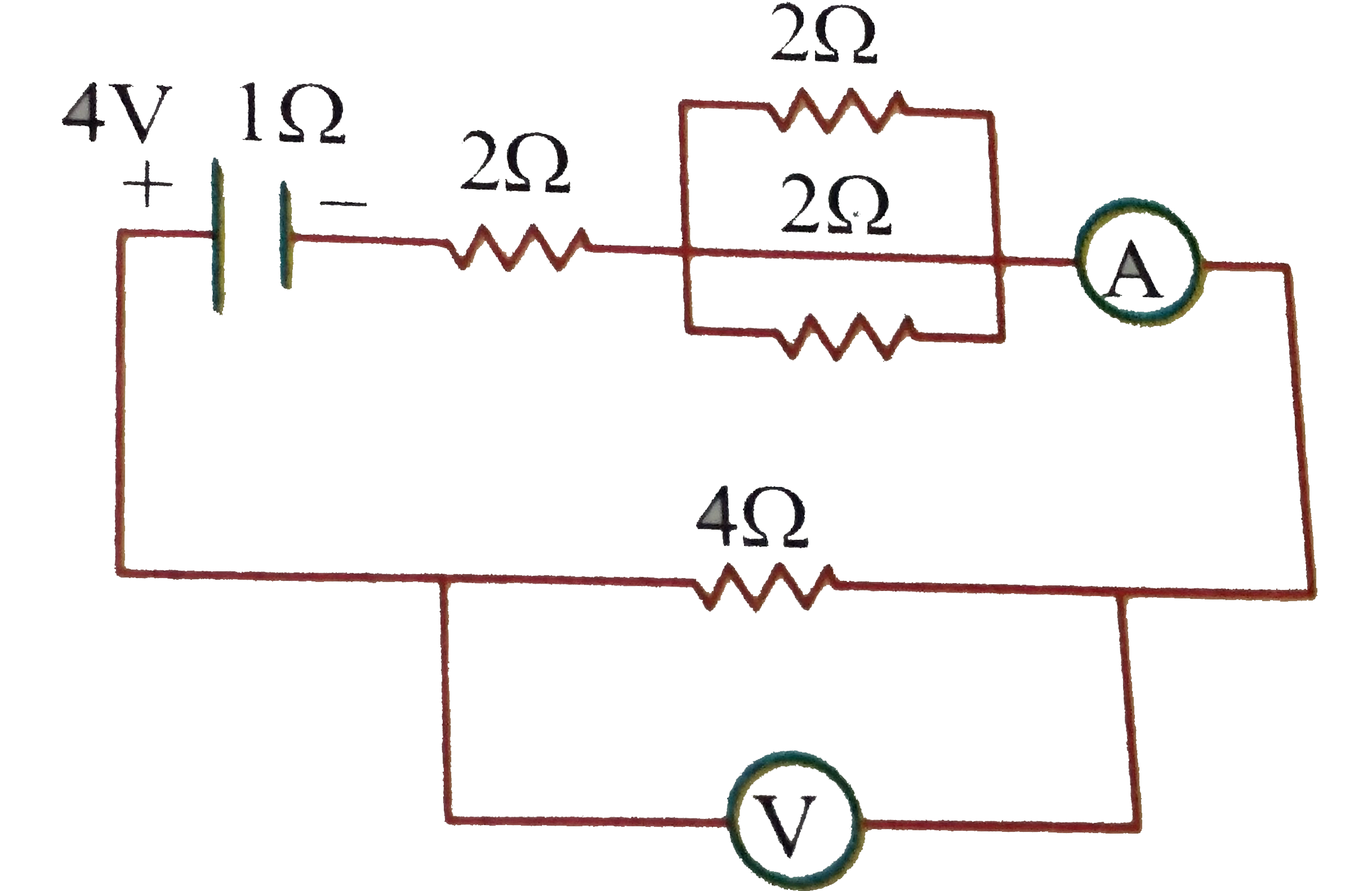
The circuit is equivalent to

NOR gate
OR gate
AND gate
NAND gate
The correct Answer is:A
Step by step video & image solution for The circuit is equivalent to by Physics experts to help you in doubts & scoring excellent marks in Class 12 exams.
Topper's Solved these Questions
- BOOK - AAKASH INSTITUTECHAPTER - SEMICONDUCTOR ELECTRONICS: MATERIALS, DEVICES AND SIMPLE CIRCUITSEXERCISE - Assignment (Section -B (Objective type question (one option is correct))29videos
SEMICONDUCTOR ELECTRONICS: MATERIALS, DEVICES AND SIMPLE CIRCUITS
- BOOK - AAKASH INSTITUTECHAPTER - SEMICONDUCTOR ELECTRONICS: MATERIALS, DEVICES AND SIMPLE CIRCUITSEXERCISE - Assignment (Section -C(Linked comprehension type question))3videos
SEMICONDUCTOR ELECTRONICS: MATERIALS, DEVICES AND SIMPLE CIRCUITS
- BOOK - AAKASH INSTITUTECHAPTER - SEMICONDUCTOR ELECTRONICS: MATERIALS, DEVICES AND SIMPLE CIRCUITSEXERCISE - Try yourself20videos
SEMICONDUCTOR ELECTRONICS: MATERIALS, DEVICES AND SIMPLE CIRCUITS
- BOOK - AAKASH INSTITUTECHAPTER - SEMICONDUCTOR ELECTRONICS (MATERIAL, DEVICES AND SIMPLE CIRUITS )EXERCISE - Assignment SECTION - D (Assertion & reason type Question)10videos
SEMICONDUCTOR ELECTRONICS (MATERIAL, DEVICES AND SIMPLE CIRUITS )
- BOOK - AAKASH INSTITUTECHAPTER - SYSTEM OF PARTICLES AND ROTATIONAL MOTIONEXERCISE - Try Yourself63videos
SYSTEM OF PARTICLES AND ROTATIONAL MOTION
Similar Questions
An n-type semi- conductor is
01:49View SolutionIn p-n junction diode, near junction holes combine with electrons, and impurity ions form a barrier potential which opposes the recombination of electron-hole pairs. Value of barriers potential for Si is 0.7 volt and for Ge is 0.3 V. thus charge density at the junction becomes zero and an electric field is produced near junction. this region is called depletion layer. Thickness of depletion layer is of the order of 10−6 meter. in forward bias p terminal is connected with the positive terminal of cell and n is connected with negative terminal of cell and n is connected with negative terminal of cell. as forward voltage is increased, current increases exponentially.
As forward voltage is increased barrier potential in p-n junction diode is02:21View SolutionIn semiconductor at a room temperature
01:30View SolutionIntrinsic semiconductor at absolute zero temperature is a
01:35View SolutionTwo bodies of masses 1kg and 3kg are lying in xy plane at (0,0) and (2,−1) respectively. What are the coordinates of the centre of mass ?
Hint. xcm=m1x1+m2x2m1+x2, ycm=m1y1+m2y2m1+m204:17View SolutionThe circuit is equivalent to
 02:08View Solution
What is the equivalent resistance of the circuit05:12View SolutionThe circuit is equivalent to
 02:51View Solution
Consider the following circuit : The equivalent resistance of the circuit will be
01:36View SolutionThe circuit is equivalent to -
 06:11View Solution
The circuit is equivalent to
01:46View SolutionSimplest circuit equivalent to the following circuit is :
 02:00View Solution
The circuit is equivalent to
 02:09View Solution
The circuit is equivalent to
 04:19View Solution
The circuit is equivalent to
 02:23View Solution
परिपथ
 समतुल्य होगा :-02:02View Solution

