In the adder circuits of two inputs
AND gate is used for carry forward memory
XOR gate is used for display
Both (1) and (2)
none of these
The correct Answer is:C
Step by step video, text & image solution for In the adder circuits of two inputs by Physics experts to help you in doubts & scoring excellent marks in Class 12 exams.
Topper's Solved these Questions
- BOOK - AAKASH INSTITUTECHAPTER - SEMICONDUCTOR ELECTRONICS: MATERIALS, DEVICES AND SIMPLE CIRCUITSEXERCISE - Assignment (Section -C(Linked comprehension type question))3videos
SEMICONDUCTOR ELECTRONICS: MATERIALS, DEVICES AND SIMPLE CIRCUITS
- BOOK - AAKASH INSTITUTECHAPTER - SEMICONDUCTOR ELECTRONICS: MATERIALS, DEVICES AND SIMPLE CIRCUITSEXERCISE - Assignment (Section-D (Assertion and reason))5videos
SEMICONDUCTOR ELECTRONICS: MATERIALS, DEVICES AND SIMPLE CIRCUITS
- BOOK - AAKASH INSTITUTECHAPTER - SEMICONDUCTOR ELECTRONICS: MATERIALS, DEVICES AND SIMPLE CIRCUITSEXERCISE - Assignment (Section -A (Objective Type question (One option is correct))50videos
SEMICONDUCTOR ELECTRONICS: MATERIALS, DEVICES AND SIMPLE CIRCUITS
- BOOK - AAKASH INSTITUTECHAPTER - SEMICONDUCTOR ELECTRONICS (MATERIAL, DEVICES AND SIMPLE CIRUITS )EXERCISE - Assignment SECTION - D (Assertion & reason type Question)10videos
SEMICONDUCTOR ELECTRONICS (MATERIAL, DEVICES AND SIMPLE CIRUITS )
- BOOK - AAKASH INSTITUTECHAPTER - SYSTEM OF PARTICLES AND ROTATIONAL MOTIONEXERCISE - Try Yourself63videos
SYSTEM OF PARTICLES AND ROTATIONAL MOTION
Similar Questions
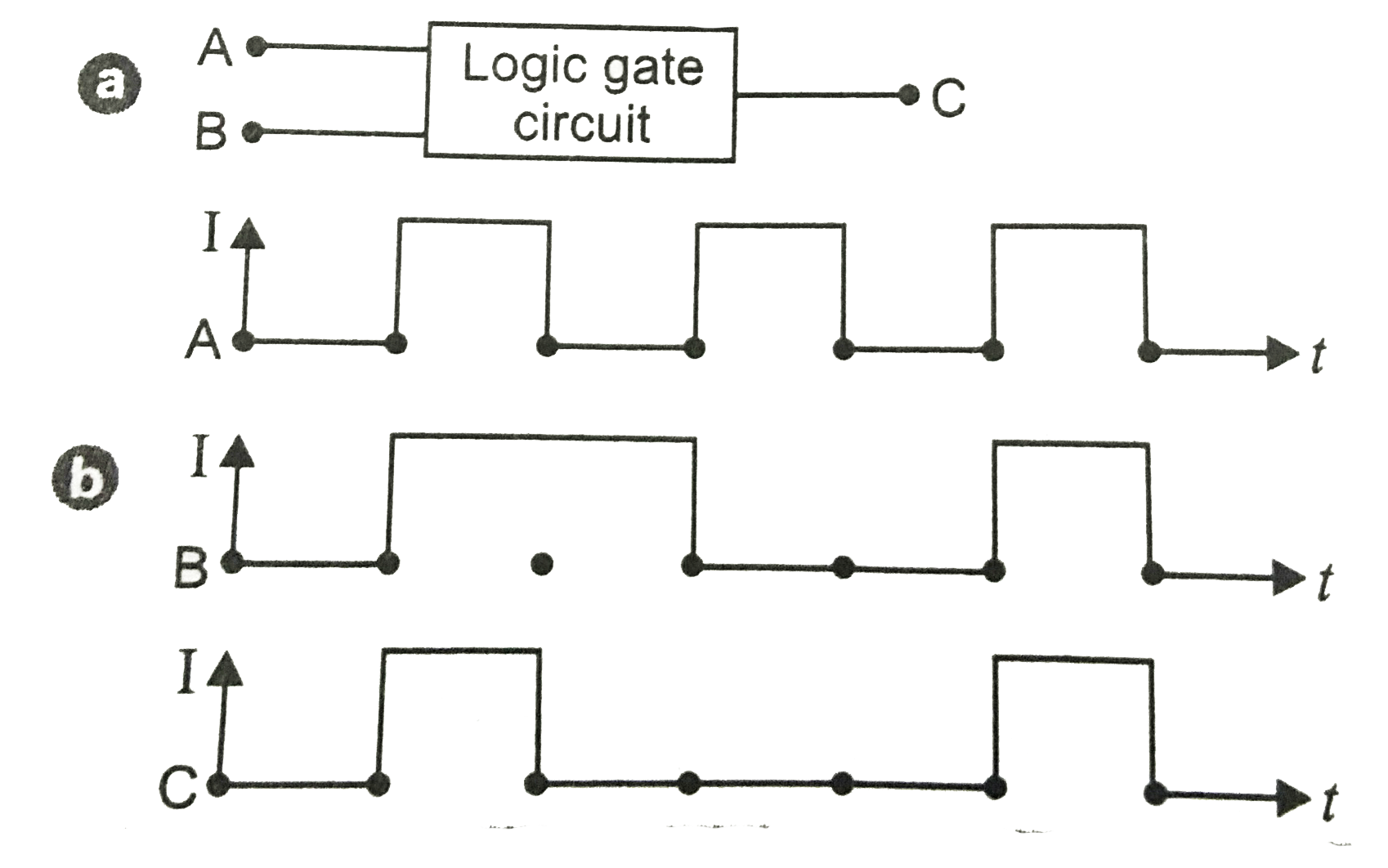
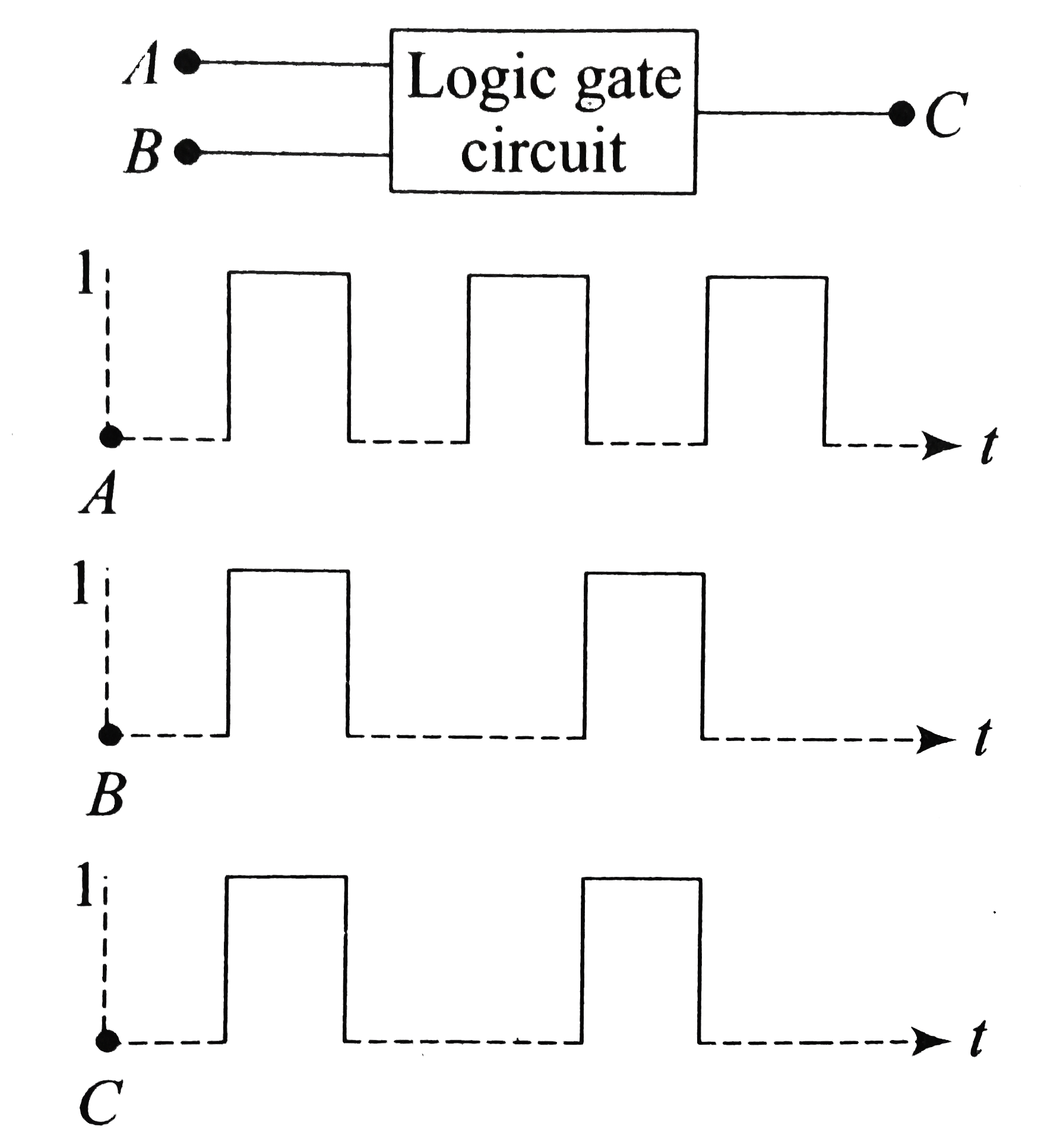
The following figure shows a logic gate circuit with two inputs A and B and the output C. The voltage waveforms of A, B and C are as shown below.
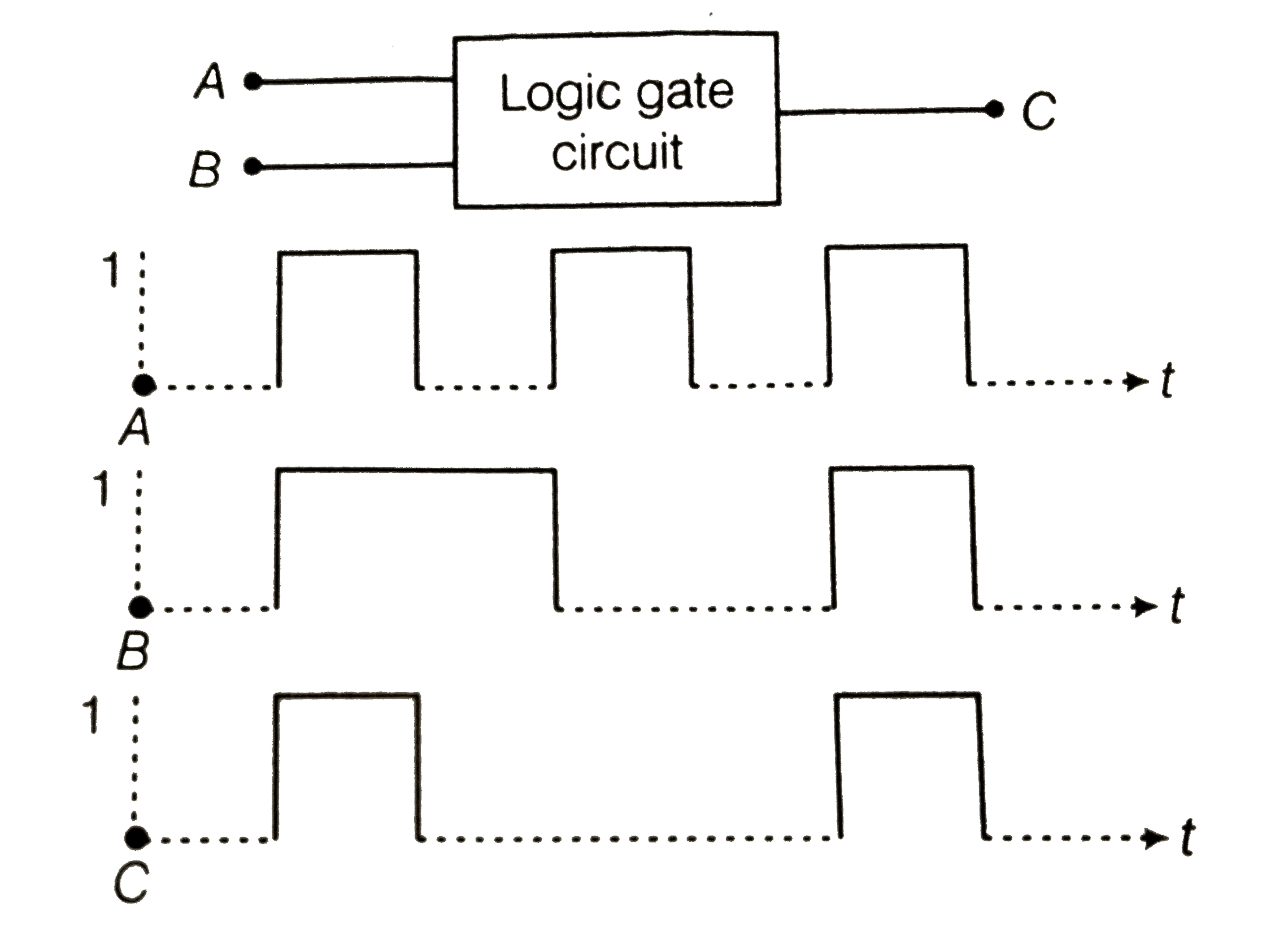
The logic circuit gate isView SolutionThe following figure showns a AND logic gate circuit with two inputs A and B and the output C. The voltage waveforms at C will be -
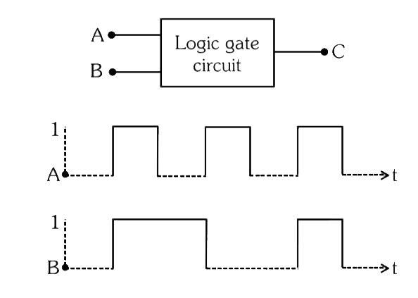 View Solution
Knowledge Check
- Question 1 - Select One
The following shows a logic gate circuit with two inputs A and B and the output C. The voltage waveforms of A, B and C are as shown below.
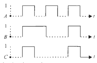
The logic circuit gate isAOR gateBAND gateCNAND gateDNOR gate - Question 2 - Select One
The following figure shows a logic gate circuit with two inputs A and B and the output C. The voltage waveforms of A, B and C are as shown below
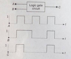
The logic circuit gate isAAND gateBNAND gateCNOR gateDOR gate - Question 3 - Select One
The following figure shows a logic gate circuit with two inputs A and B and the output C. The voltage waveforms of A, B and C are as shown below

The logic circuit gate isAAND gateBNAND gateCNOR gateDOR gate
The Fig.shows a logic gate circuit with two inputs A and B and the output C are as shown in Fig.
 View Solution
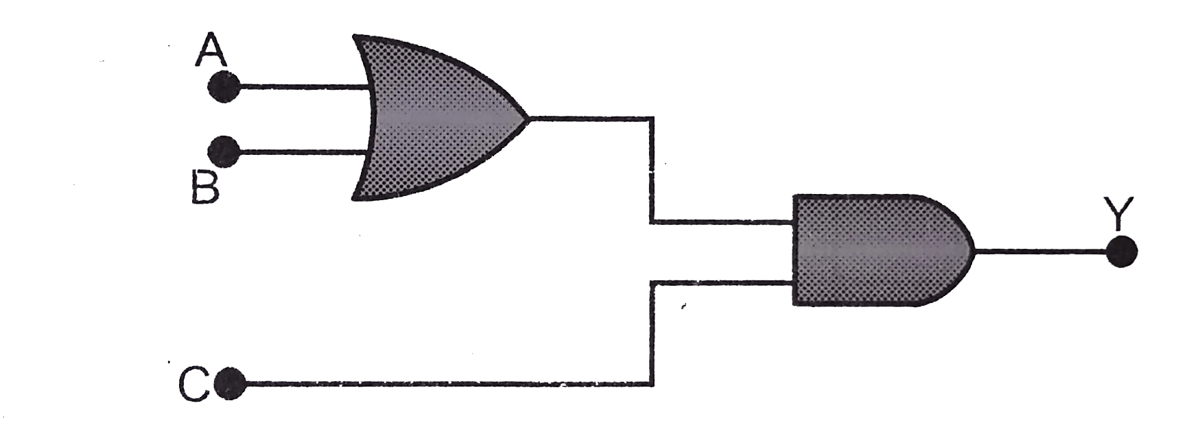
In order to obtain an output Y=1 form the circuit of fig. the inputs must be
 View Solution
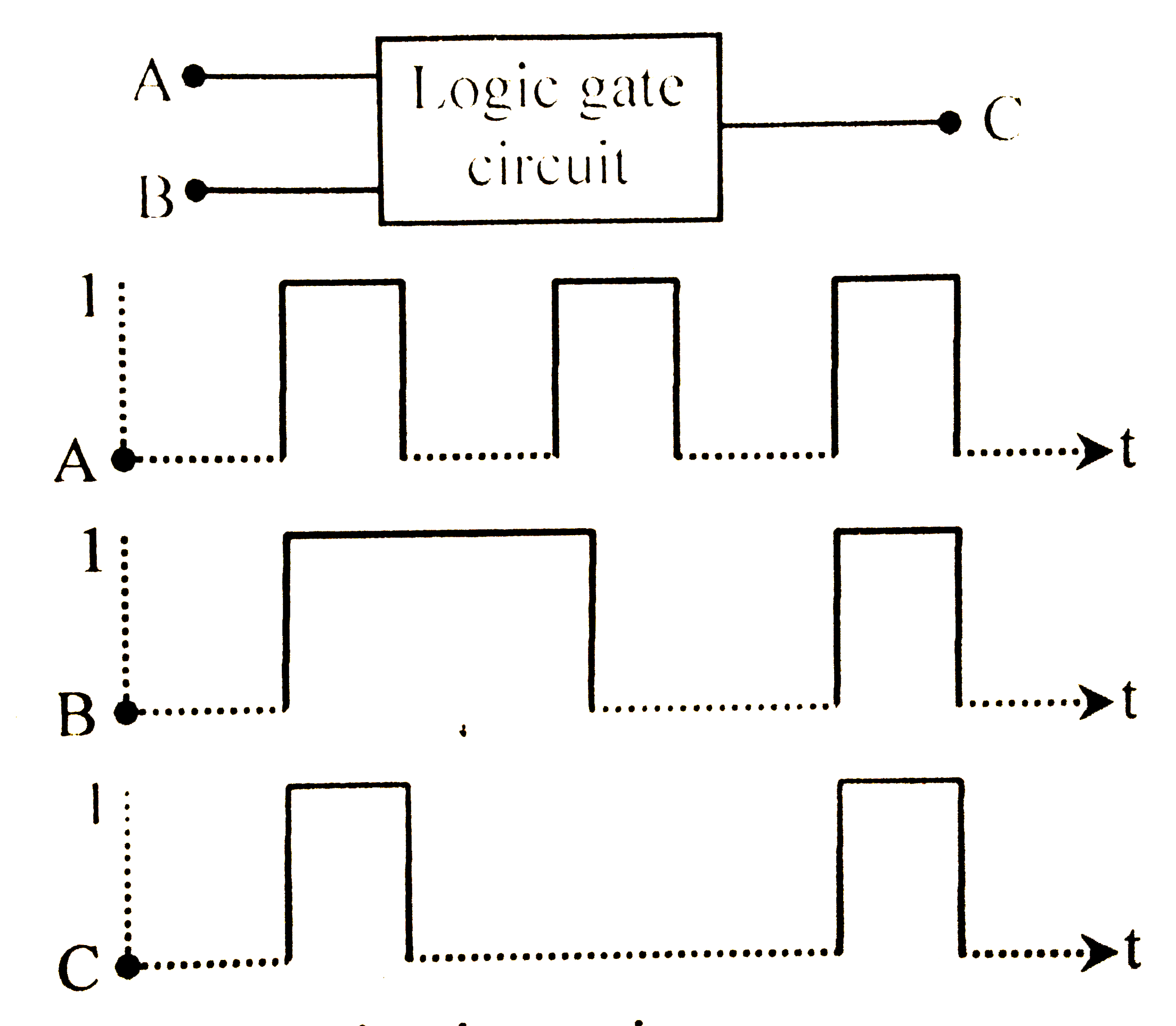
The following figure shows a logic gate circuit with two inputs A and B and the output C. The voltage waveforms of A, B and C are as shown below-
 View Solution
The following figure shows a logic gate circuit with two inputs A and B and the output Y. The voltage waveforms of A,B and Y are as given :
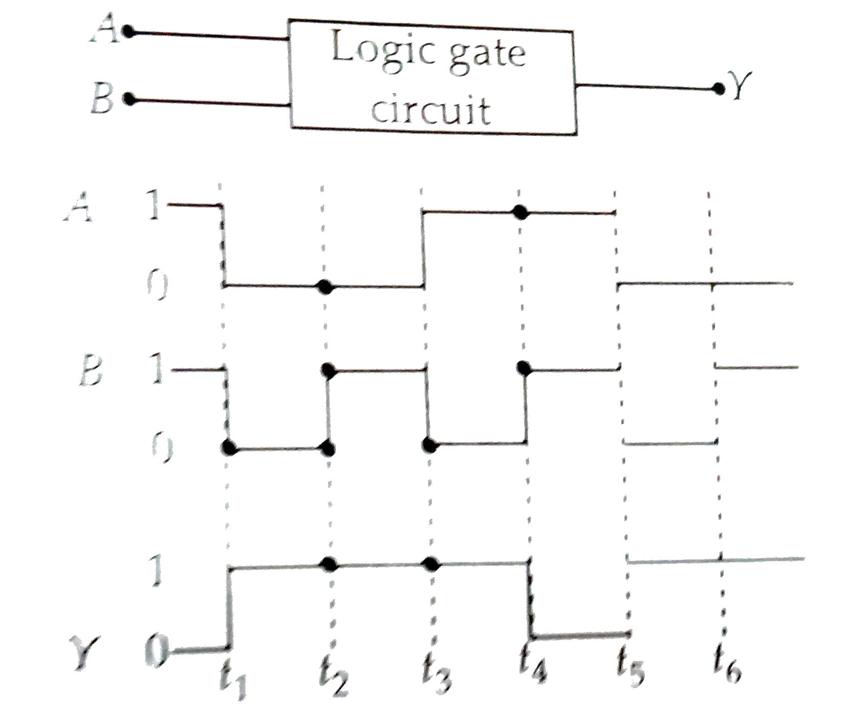
The logic gate isView SolutionThe following figure shows a logic gate circuit with two inputs A and B and the output C. The voltage waveforms of A,B and C are as shown below
 View Solution

