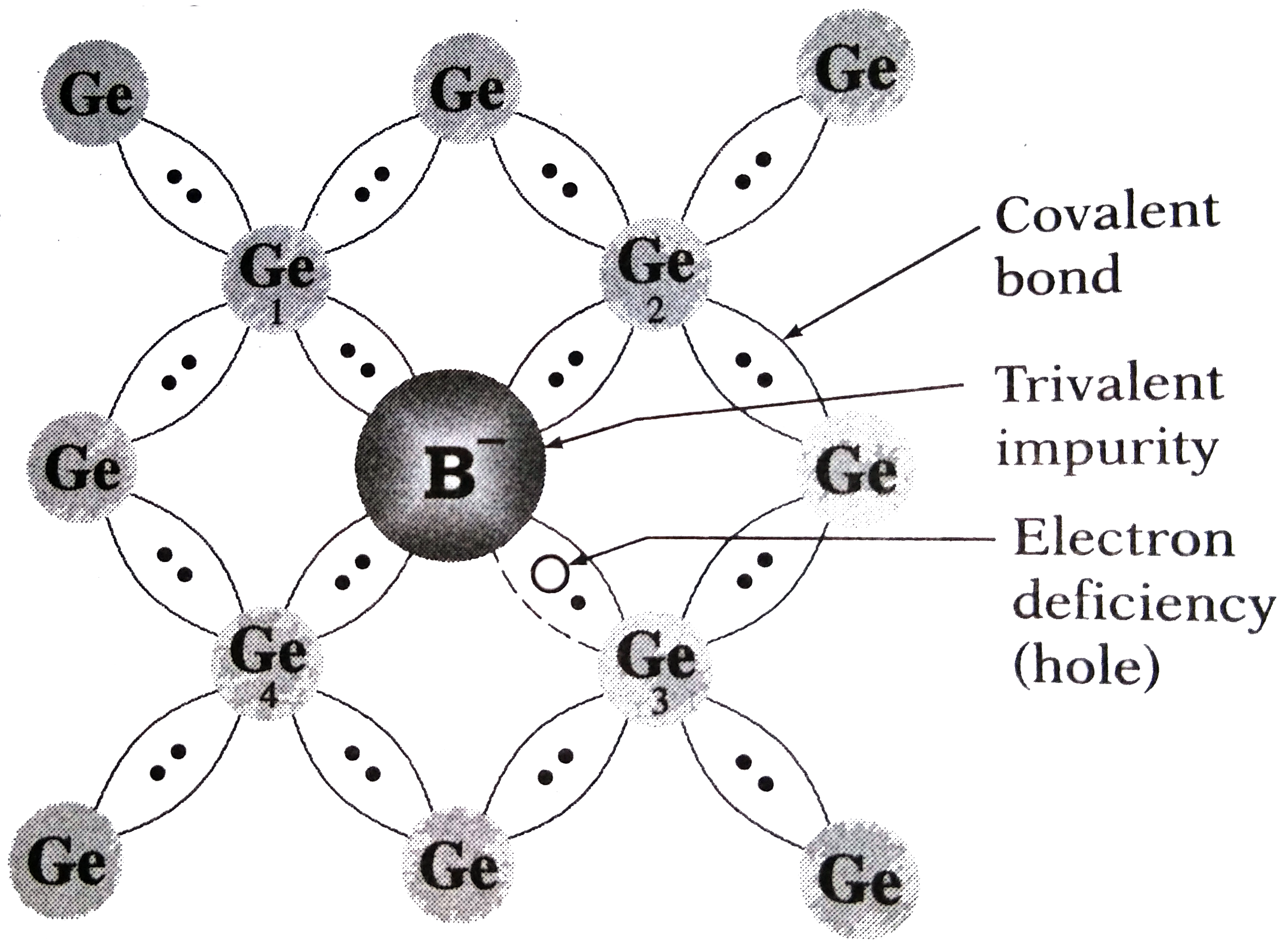
With a neat labelled diagram of the structure, explain formation of a p-type semiconductor.
Text Solution
(1) A trivalent element such as boron, gallium or aluminiom has three valence electrons. Silicon and germanium are tetravalent elements.

A p-type semiconductor is formed when crystal of tetravalent sillicon or germanium is doped with a trivalent impurity.
(2)All the three valence electrons of an impurity atom form covali bonds with three of the four nearest-neighbour ost anoms. One bonds remains incomplete and needs an additional electron.
(3) A valence electron of a meighbouring atom may become free and electrons to the condaction band. Such mpurity holes greatly inrease the small concentration of holes that are already present in the material due thermal energy. The total hole concentration in the valence band greatly exceeds that of thermal electrons in the conduction band : . Conduction in such an extrinsic semiconductor is largely due to holes.
(4) Such an extrinsic semiconductor is, therefore, termed positive charge carrier types, or p-type, semiconductor.
|
Topper's Solved these Questions
- EXPLANATION, CHARACTERISTICS AND PROPERTIES BOOK - NAVNEET PUBLICATION - MAHARASHTRA BOARDCHAPTER - EXPLANATION, CHARACTERISTICS AND PROPERTIES EXERCISE - Communication Systems
7 Videos
- EXPLANATION, CHARACTERISTICS AND PROPERTIES BOOK - NAVNEET PUBLICATION - MAHARASHTRA BOARDCHAPTER - EXPLANATION, CHARACTERISTICS AND PROPERTIES EXERCISE - Assignments
2 Videos
- EXPLANATION, CHARACTERISTICS AND PROPERTIES BOOK - NAVNEET PUBLICATION - MAHARASHTRA BOARDCHAPTER - EXPLANATION, CHARACTERISTICS AND PROPERTIES EXERCISE - Atoms, Molecules and Nuclei
6 Videos
- EXPERIMENTS AND DIAGRAMSBOOK - NAVNEET PUBLICATION - MAHARASHTRA BOARDCHAPTER - EXPERIMENTS AND DIAGRAMSEXERCISE - ATOMS, MOLECULES AND NUCLEI
1 Videos
- INSTRUMENTS : CONSTRUCTION AND WORKING BOOK - NAVNEET PUBLICATION - MAHARASHTRA BOARDCHAPTER - INSTRUMENTS : CONSTRUCTION AND WORKING EXERCISE - Semiconductors
6 Videos
Similar Questions
Draw a neat and labelled diagram showing the structure of an atom.
View SolutionWith a neat labelled diagram, explain how a rainbow is formed.
View SolutionDraw neat labelled diagrams : Type of lenses.
View SolutionWith neat and labelled diagram, explain froth floatation method.
View SolutionWith a neat labelled diagram, explain the working of a refracting telescope.
View SolutionExplain oogenesis with the help of a neat labelled diagram
View SolutionExplain about Bichromate cell with a neat labelled diagram.
View SolutionExplain about Bichromate cell with a neat labelled diagram.
View SolutionExplain mechanism of breathing with neat labelled diagram.
View SolutionExplain in brief the mechanism of antibody antigen complexed formation with a neat labelled diagram.
View Solution
