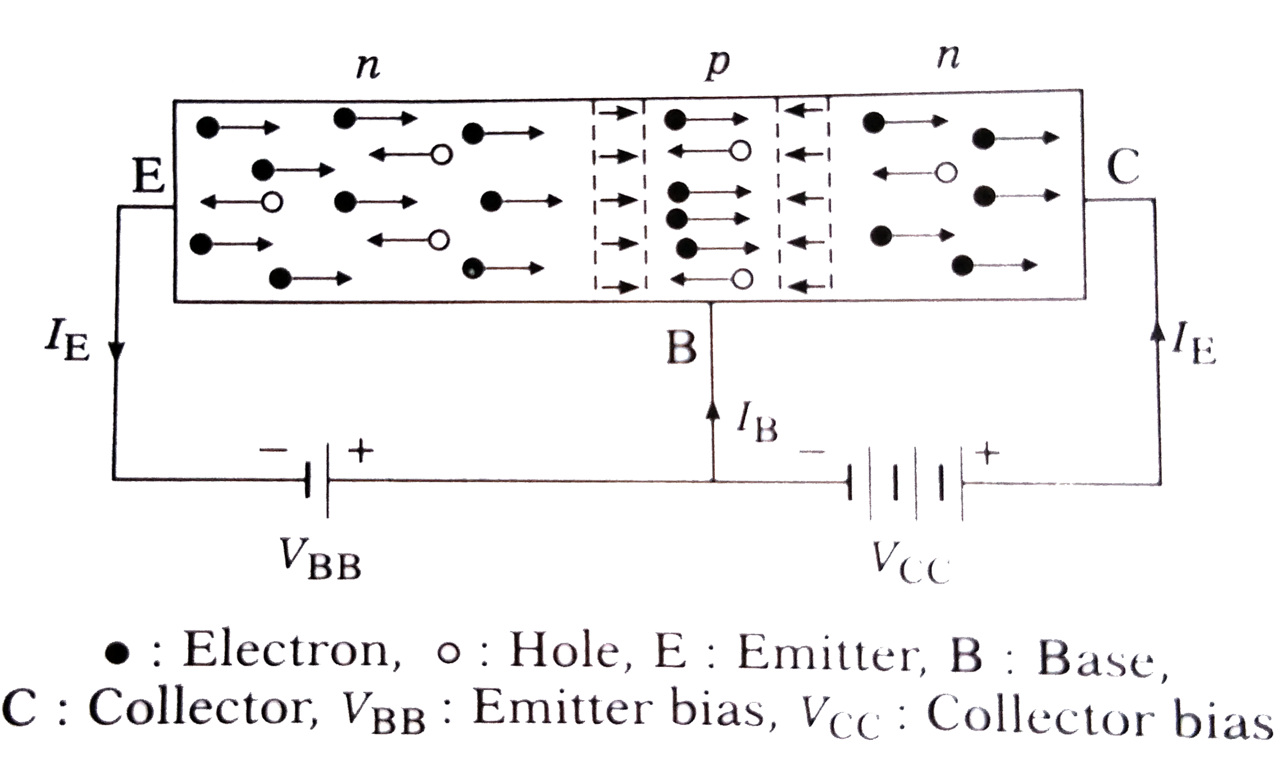
Explain the conduction process in a junction transistor with a neat labelled diagram.
For normal operation of a junction transistor, the emitter-base junction is always forward biased and the collector-base junction is always reverse biased. Consider the more common npn transistor. The emitter. base junction is forward biased by the battery VBB While the collector-base junction is reverse biased by the battery VCC. The base is common, so that the junction in opposite directions. This current is called the reverse curran npn transistor in common base configuration. neat labelled diagram. the circuit shown is called the common-base configuration.
The emitter is a very heavily doped n-type region. Hence, the current between emitter E and base B is almost entirely electron current from E into B across the forward biased emitter junction.
The ρ-type base is narrow and the hole density in the base is very low. Therefore, practically all the injected electrons diffuse right across the base to the collector junction without recombining with holes. Since this collector-base junction is reverse-baised, the electrons on reaching this junction are quickly swept into the n-type collector region, where they constitute the collector current IC.
In practice, about 1% to 5% of the holes from the emitter recombine with holes in the base year layer and cause a small current IB to flow in the base lead. Therefore, the emitter current, IE=IB+IC
If a pnp transistor is used, the battery connections must be reversed for the correct bias. The conduction process is similar but takes place instead by migration of holes from the emitter to collector.

Topper's Solved these Questions
- EXPLANATION, CHARACTERISTICS AND PROPERTIES BOOK - NAVNEET PUBLICATION - MAHARASHTRA BOARDCHAPTER - EXPLANATION, CHARACTERISTICS AND PROPERTIES EXERCISE - Communication Systems
7 Videos
- EXPLANATION, CHARACTERISTICS AND PROPERTIES BOOK - NAVNEET PUBLICATION - MAHARASHTRA BOARDCHAPTER - EXPLANATION, CHARACTERISTICS AND PROPERTIES EXERCISE - Assignments
2 Videos
- EXPLANATION, CHARACTERISTICS AND PROPERTIES BOOK - NAVNEET PUBLICATION - MAHARASHTRA BOARDCHAPTER - EXPLANATION, CHARACTERISTICS AND PROPERTIES EXERCISE - Atoms, Molecules and Nuclei
6 Videos
- EXPERIMENTS AND DIAGRAMSBOOK - NAVNEET PUBLICATION - MAHARASHTRA BOARDCHAPTER - EXPERIMENTS AND DIAGRAMSEXERCISE - ATOMS, MOLECULES AND NUCLEI
1 Video
- INSTRUMENTS : CONSTRUCTION AND WORKING BOOK - NAVNEET PUBLICATION - MAHARASHTRA BOARDCHAPTER - INSTRUMENTS : CONSTRUCTION AND WORKING EXERCISE - Semiconductors
6 Videos
Similar Questions
Explain about Bichromate cell with a neat labelled diagram.
View SolutionExplain about Bichromate cell with a neat labelled diagram.
View SolutionExplain mechanism of breathing with neat labelled diagram.
View SolutionExplain processing of hn-RNA with the help of neat and labelled diagram.
View SolutionExplain magnetic separation process of ores with the help of a neat , labelled diagram.
View SolutionExplain oogenesis with the help of a neat labelled diagram
View SolutionExplain hydraulic separation method with neat and labelled diagram
View SolutionExplain the process of production of edible vaccines with a neat diagram.
View SolutionExplain in brief the mechanism of antibody antigen complexed formation with a neat labelled diagram.
View SolutionExplain the structure of root hair with the help of neat and labelled diagrams.
View Solution
