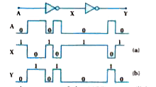
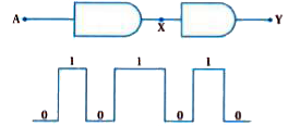
A logic circuit is shown in the diagram. Draw the output signal at the point X and Y for the input signal shown in the figure at point A.
 Solution in Gujrati


The correct Answer is:D
At the forward bias connection of p-n junction from RL value of input signal is 5V in output. For input signal -5V negative voltage of input we are not getting output.
∴ (D) is correct option.
Topper's Solved these Questions
- SEMICONDUCTOR ELECTRONICS : MATERIALS, DEVICES AND SIMPLE CIRCUITS BOOK - KUMAR PRAKASHANCHAPTER - SEMICONDUCTOR ELECTRONICS : MATERIALS, DEVICES AND SIMPLE CIRCUITS EXERCISE - Section-D : Multiple Choice Questions (MCQs) (MCQs From .DARPAN. Based On Textbook)
116 Videos
- SAMPLE QUESTION PAPER BOOK - KUMAR PRAKASHANCHAPTER - SAMPLE QUESTION PAPER EXERCISE - PART-B SECTION-C
5 Videos
- WAVE OPTICSBOOK - KUMAR PRAKASHANCHAPTER - WAVE OPTICSEXERCISE - SECTION-D (MULTIPLCE CHOICE QUESTIONS (MCQS)) (MCQS FROM DARPAN BASED ON TEXTBOOK)
239 Videos
Similar Questions
Which of the following is not a conductor of electricity?
View SolutionTwo charges –q and +q are located at points (0, 0, –a) and (0, 0, a), respectively.
(a) What is the electrostatic potential at the points (0, 0, z) and (x, y, 0) ?
(b) Obtain the dependence of potential on the distance r of a point from the origin when r/a>>1 .
(c) How much work is done in moving a small test charge from the point (5,0,0) to (–7,0,0) along the x-axis? Does the answer change if the path of the test charge between the same points is not along the x-axis?
View SolutionAccording to particle theory of light what is the velocity of light in a dense medium, compared to that in rare medium ?
View SolutionThe output (X) of the logic circuit shown in figure will be
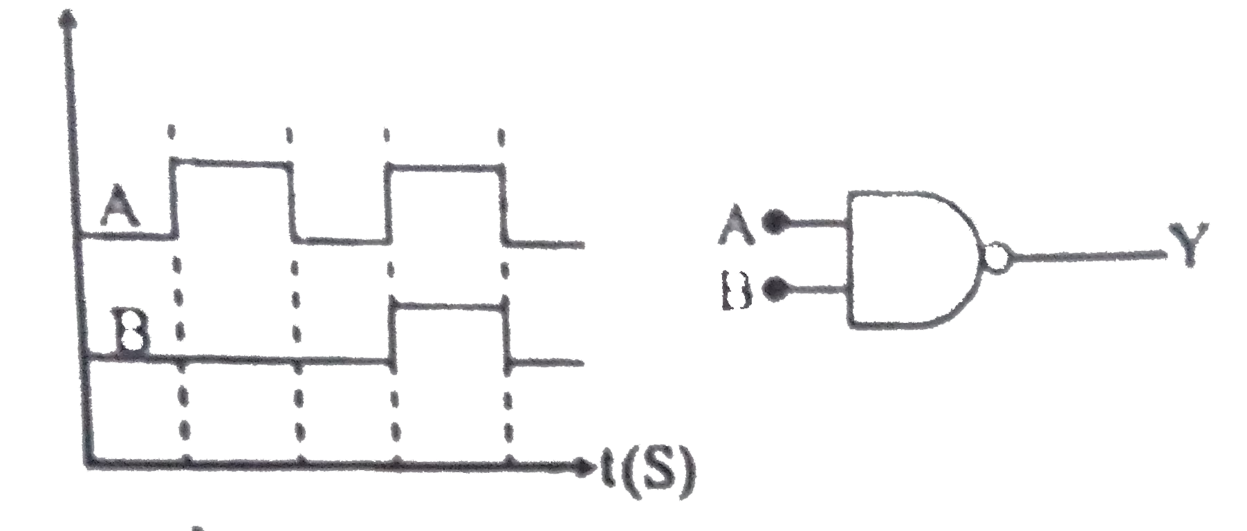
View SolutionThe real time variation of input signals A & B are as shown below. If the inputs are into NAND gate, then select the output signals from the following-
View Solutionचित्र में दिए गये गेटों P तथा Q के नाम बताइए तथा निर्गत सिग्नल Y की सत्यता सारणी बनाइए तथा निवेशी तथा निर्गत सिग्नलों के तरंग प्रतिरूप दर्शाइए ।

View SolutionThe output (X) of the logic circuit shown in figure will be
View Solutionदिये गये चित्र में AND गेट के लिए A व B निवेशी सिग्नल प्रदर्शित हैं। इसका निर्गत सिग्नल खींचिए तथा लॉजिक गेट की सतत् सारणी लिखिए।
View Solution
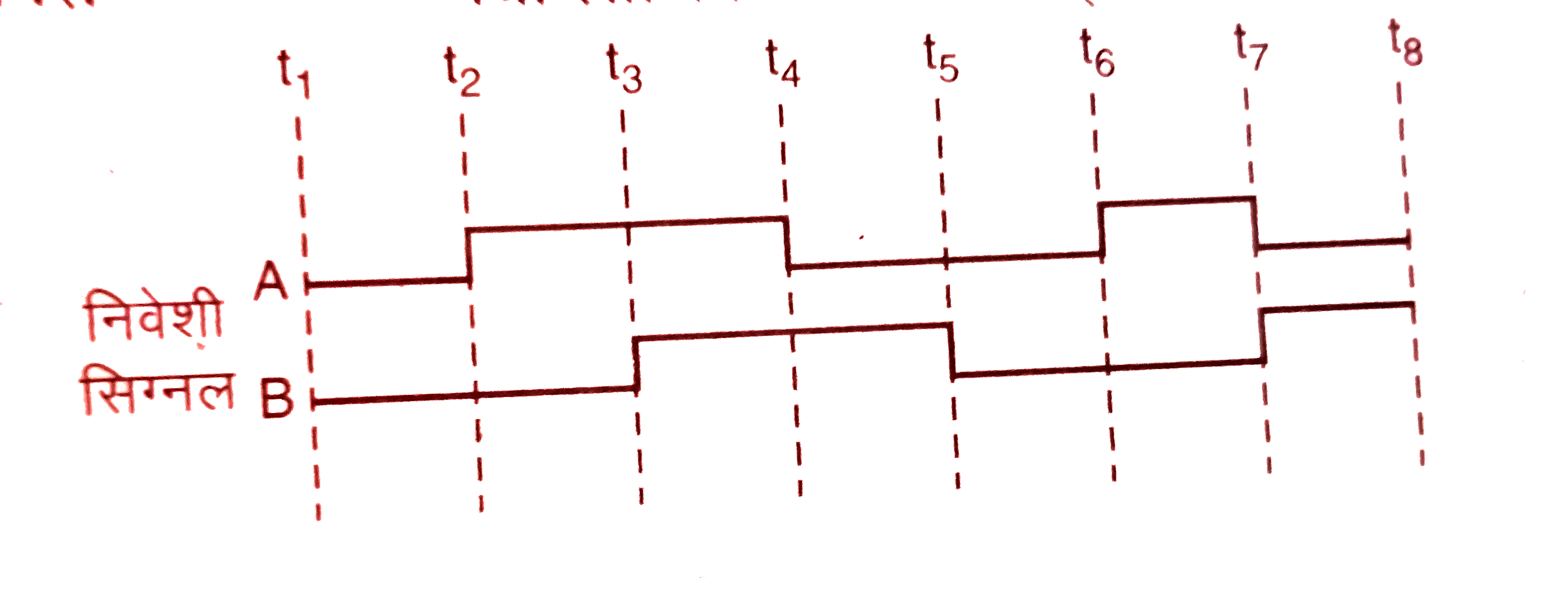
input are given as shown
then output signal is-
View SolutionThe output (X) of the logic circuit shown in figure will be
View SolutionA logic circuit is shown in the diagram. Draw the output signal at the point X and Y for the input signal shown in the figure at point A.

View SolutionA circuit of logic gte made from two AND gate is shown in following figure. Draw output waves for point X. For A and for Y.
View SolutionThe figure shows the input signal A, input signal B and output signal Y. Which logic gate does it represent ?
View Solutionनीचे दिए हुए चित्र में एक तार्किक द्वार का संकेत तथा दो निवेशी संकेत A व B दर्शाये गये है।

निर्गत तरंग संकेत बनाइये।
View Solution
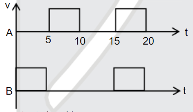
input are given as shown

then output signal is-
View SolutionThe output Y of the logic circuit as shown in figure is
View Solution
