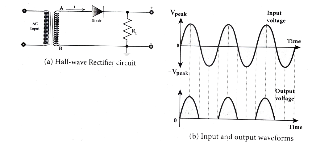
Draw the circuit diagram of a half wave rectifier and explain its working. Solution in Tamil
The half wave rectifier circuit. The circuit consists of a transformer, a p-n junction diode and a resistor. In a half wave rectifier circuit, either a positive half or the negative half of the AC input is passed through while the other half is blocked. Only one half of the input wave reaches the output. Therefore, it is called half wave rectifier. Here, a p-n junction diode acts as a rectifying diode.

During the positive half cycle:
When the positive half cycle of the ac input signal passes through the circuit, terminal A becomes positive with respect to terminal B. The diode is forward biased and hence it conducts. The current flows through the load resistor RL and the AC voltage developed across RL constitutes the output voltage V0 and the waveform of the diode current. During the negative half cycle: When the negative half cycle of the ac input signal passes through the circuit, terminal A is negative with respect to terminal B. Now the diode is reverse biased and does not conduct and hence no current passes through RL. The reverse saturation current in a diode is negligible. Since there is no voltage drop across RL the negative half cycle of ac supply is suppressed at the output.
The output of the half wave rectifier is not a steady de voltage but a pulsating wave. This pulsating voltage is not sufficient for electronic equipments. A constant or a steady voltage is required which can be obtained with the help of filter circuits and voltage regulator circuits. Efficiency (η) is the ratio of the output dc power to the ac input power supplied to the circuit. Its value for half wave rectifier is 40.6 %
Topper's Solved these Questions
Similar Questions
Write down Coulomb 's law in vector form and mention what each term represents .
View SolutionDerive an expression for electrostatic potential energy of the dipole in a uniform electric field .
View SolutionDefine capacitance . Give its unit.
View SolutionExplain the formation of depletion layer and potential barrier in p-n junction.
Draw the circuit diagram of a half wave rectifier and explain its working.
View SolutionDraw the circuit diagram of a half wave rectifier and explain its working.
View SolutionDraw the circuit diagram of half wave rectifier, showing input and output voltages.
View SolutionDraw the circuit diagram of a half wave rectifier and explain its working.
View SolutionDraw the circuit diagram of a full wave rectifier. Explain its working showing its input and output waveforms.
View SolutionWhat is a rectifier ? With suitable circuit describe the action of a full wave rectifier by drawing input and output waveforms.
View SolutionExplain the formation of depletion layer and potential barrier in p-n junction.
Draw the circuit diagram of a half wave rectifier and explain its working.
View SolutionDraw the circuit diagram of a half-wave rectifier. Explain its working. What is the frequency of ripple in its output?
View SolutionDraw a neat diagram of a full wave rectifier and explain its working
View SolutionDraw a circuit diagram of a full rectifier and explain its working.
View SolutionDraw the circuit diagram of half wave rectifier.
View SolutionDraw the circuit diagram of a half wave rectifier. Hence explain its working.
View Solution
