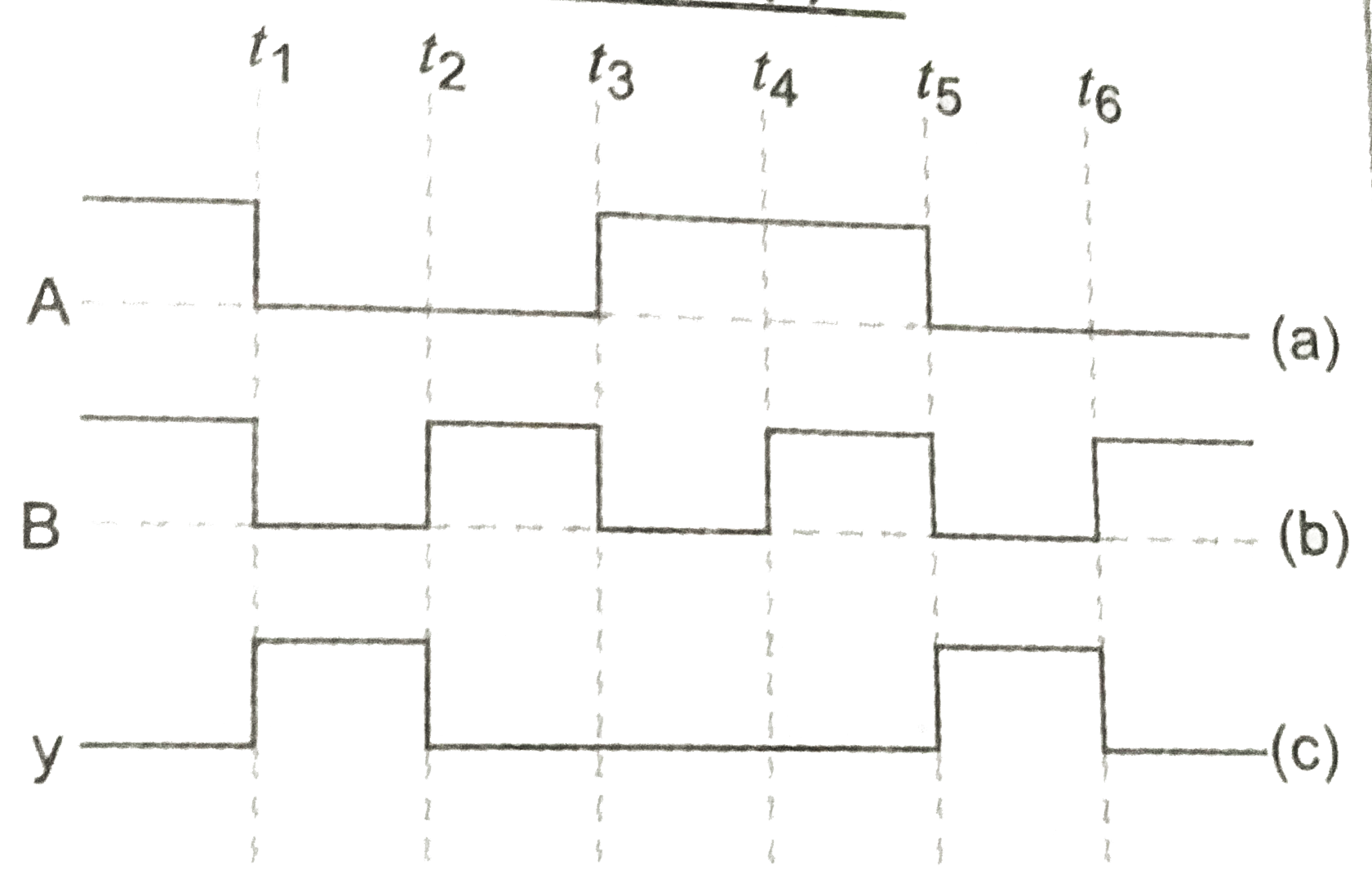
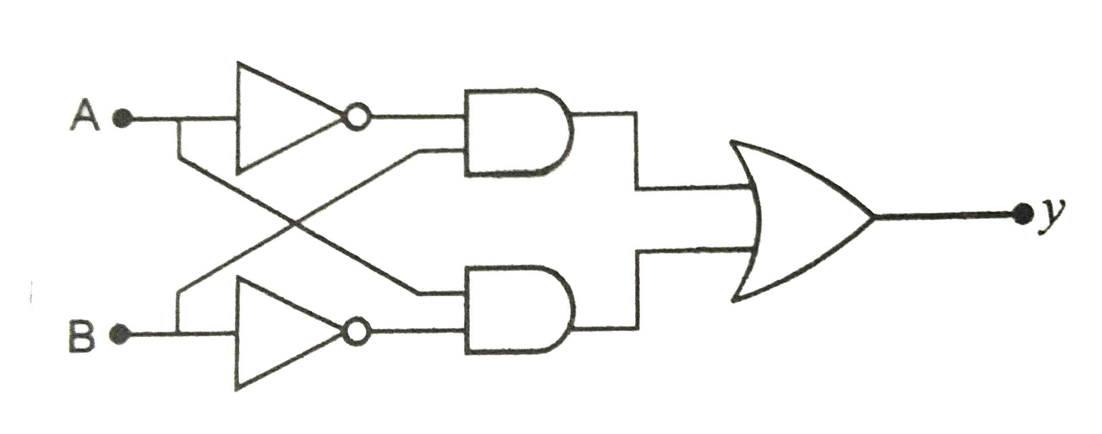
Explain how an OR gate may be constructed with AND and NOT gates. A logic circuit is given in the Fig.charge it in simpler form.
![Explain how an OR gate may be constructed with AND and NOT gates. A logic circuit is given in the Fig.charge it in simpler form. [Refer to conceptual Problem 4 for first part. The given figure represents AND gates as y=A.(barA(A+B))=A.barA+A.B=A.B]](https://d10lpgp6xz60nq.cloudfront.net/physics_images/PR_XII_V02_C09_E01_068_Q01.png)
[Refer to conceptual Problem 4 for first part. The given figure represents AND gates as y=A.(¯¯¯A(A+B))=A.¯¯¯A+A.B=A.B]
Step by step video & image solution for Explain how an OR gate may be constructed with AND and NOT gates. A logic circuit is given in the Fig.charge it in simpler form. [Refer to conceptual Problem 4 for first part. The given figure represents AND gates as y=A.(barA(A+B))=A.barA+A.B=A.B] by Physics experts to help you in doubts & scoring excellent marks in Class 12 exams.
Updated on:21/07/2023Topper's Solved these Questions
- ELECTRONIC DEVICESBOOK - PRADEEPCHAPTER - ELECTRONIC DEVICESEXERCISE - LONG QUESTION ANSWER
2 Videos
- ELECTRONIC DEVICESBOOK - PRADEEPCHAPTER - ELECTRONIC DEVICESEXERCISE - PROBLEMS FOR PRACTICE
7 Videos
- ELECTRONIC DEVICESBOOK - PRADEEPCHAPTER - ELECTRONIC DEVICESEXERCISE - HIGHER ORDER THINKING SKILLS
1 Videos
- ELECTROMAGNETIC WAVESBOOK - PRADEEPCHAPTER - ELECTROMAGNETIC WAVESEXERCISE - II Focus multiple choice question
5 Videos
- ELECTROSTATICSBOOK - PRADEEPCHAPTER - ELECTROSTATICSEXERCISE - ASSERTION-REASON TYPE QUESTIONS
2 Videos
Similar Questions
Knowledge Check
The Fig.shows a logic gate circuit with two inputs A and B and the output C are as shown in Fig.
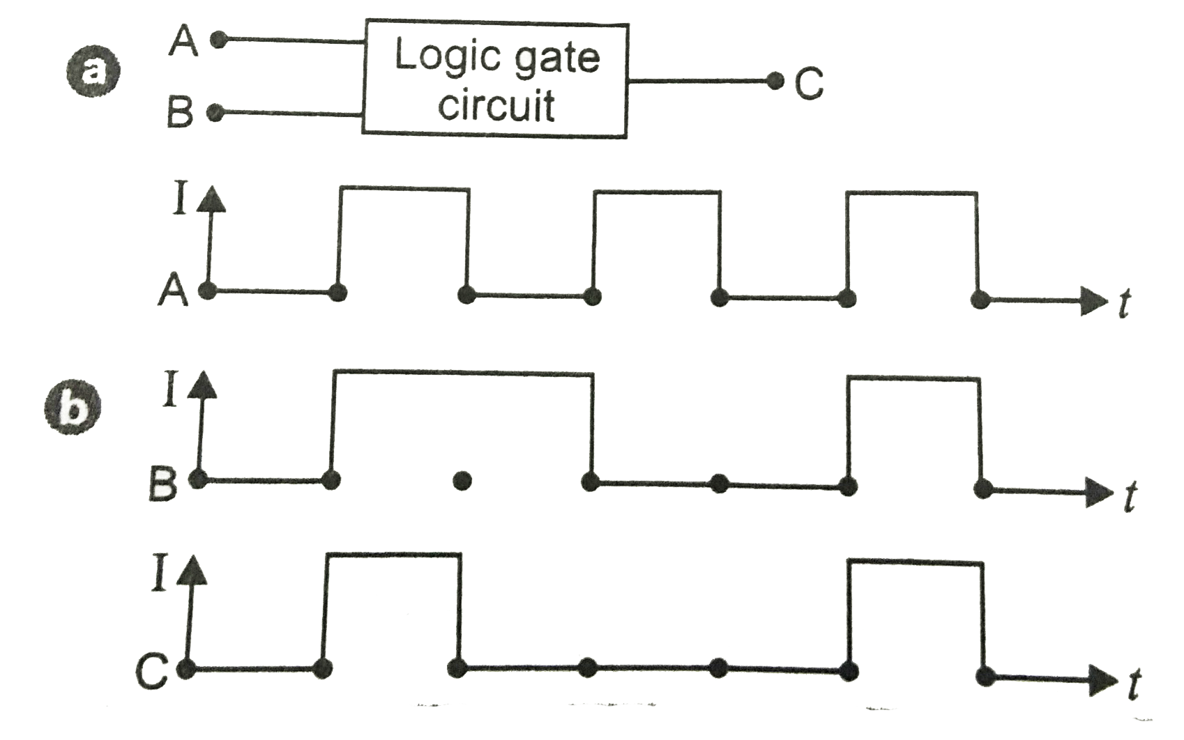 AOR gateBAND gateCNAND gateDNOR gate
Logic gate for input A and B is given in figure
_2019_CBT7_E01_022_Q01.png)
Which table is correct for given gates system.A∣∣ ∣ ∣ ∣ ∣ ∣∣ABY000101010111∣∣ ∣ ∣ ∣ ∣ ∣∣B∣∣ ∣ ∣ ∣ ∣ ∣∣ABY000101011110∣∣ ∣ ∣ ∣ ∣ ∣∣C∣∣ ∣ ∣ ∣ ∣ ∣∣ABY001100011110∣∣ ∣ ∣ ∣ ∣ ∣∣D∣∣ ∣ ∣ ∣ ∣ ∣∣ABY001101010110∣∣ ∣ ∣ ∣ ∣ ∣∣Name the gate , which represents the Boolean expression y = A. B for inputs A, B
AANDBNORCNANDDNOT
Sketch the output Y from NAND gate having input A A and B given below, Fig.
View SolutionUsing the wave forms of the input A and B, draw the output waveform of the given logic circuit . Identify the logic gate obtained . Write also the truth table.

View SolutionIdentify the logic gate equivalent to the circuit shown in the Fig.Draw the truth table for all possible values of inputs A and B.
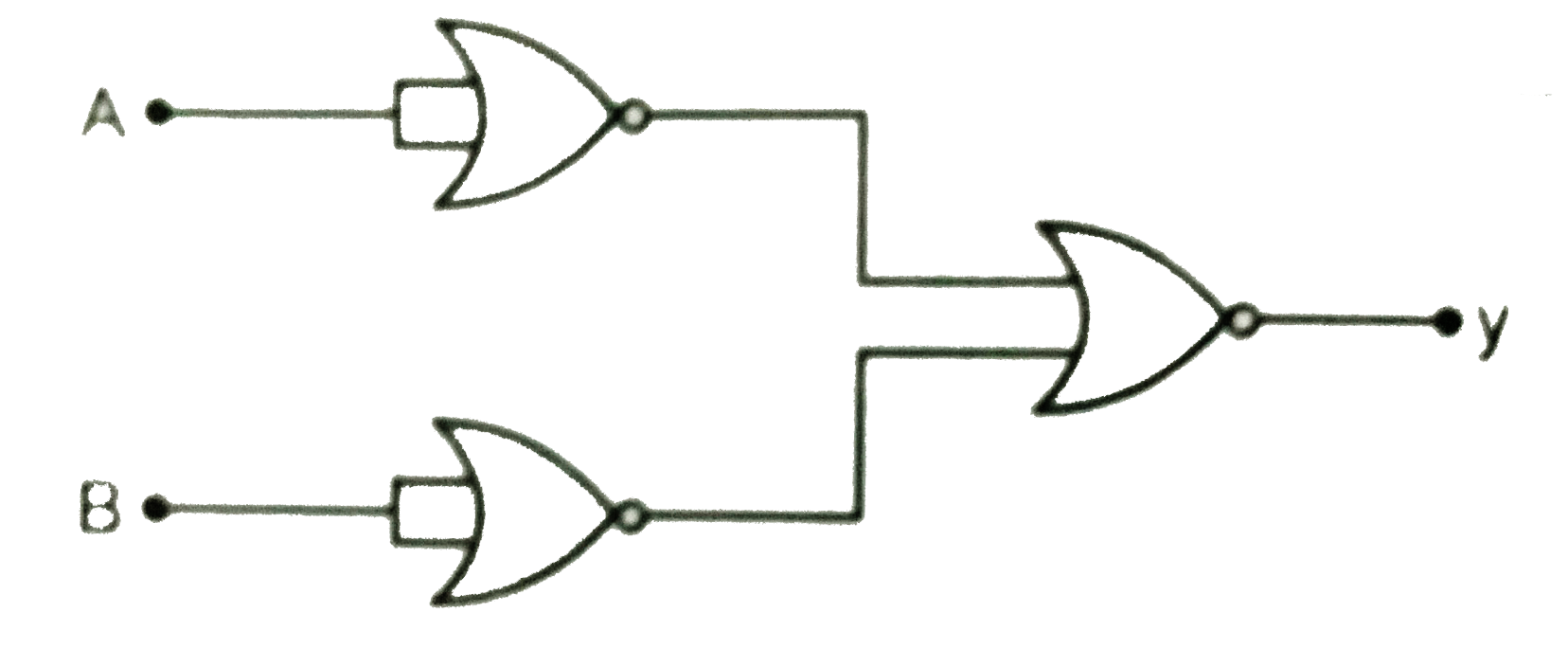
View SolutionThe following figure shown a logic gate circuit with ttwo inputs A and B and the C are as shown below
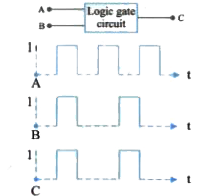
The logic circuit gate is
View SolutionThe figure shows the voltage waveforms across two inputs A and B and the output Y of a logic circuit. The logic circuit gate is
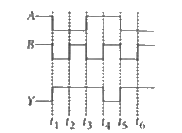
View Solution

