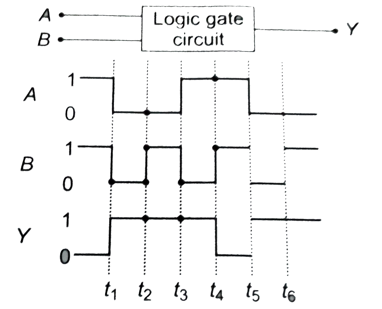
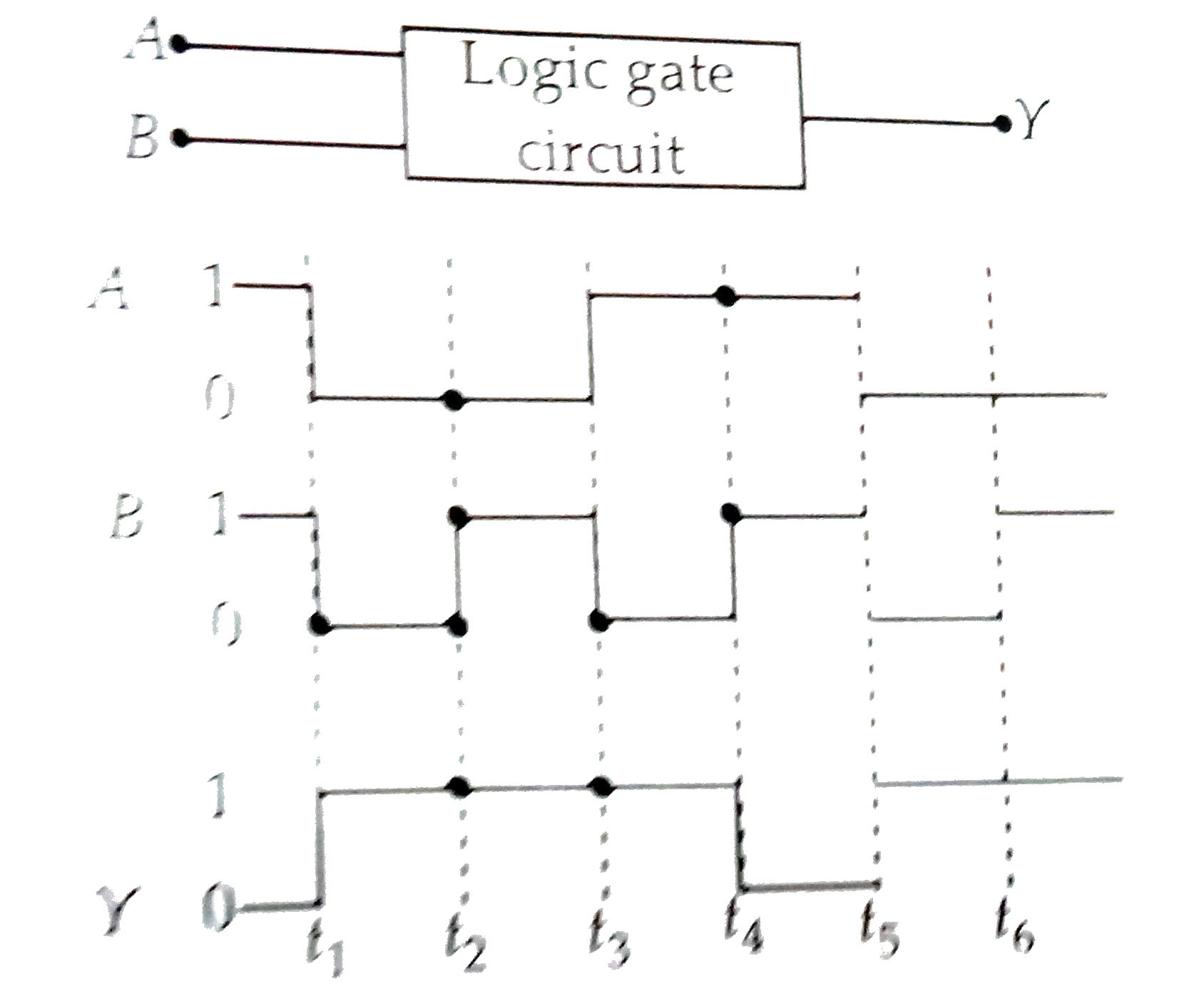
The following figure shows a logic gate circuit with two inputs A and B and the output Y. The voltage waveforms of A,B and the output Y are as given
NOR gate
OR gate
AND gate
NAND gate
The correct Answer is:D
For the given logic gate circuit, the input values of A, B and output value y are given as following:
For time 0 "to" t1,A=1,B=1,y=0
For time t1tot2,A=0,B=0,y=1
For time t2tot3,A=0,B=1,y=1
For time t3tot4,A=1,B=0,y=1
For time t4tot5,A=1,B=1,y=0
For time t5tot6,A=0,B=0,y=1
For time t to t6,A=0,B=1,y=1
From above we note that output y is low when both the input are high, otherwise it is high. It satisfies the Boolean expression, ¯¯¯¯¯¯¯¯A.B=y, which is for NAND gates. Thus logic circuit is NAND gate.
Topper's Solved these Questions
- ELECTRONIC DEVICESBOOK - PRADEEPCHAPTER - ELECTRONIC DEVICESEXERCISE - LONG QUESTION ANSWER
2 Videos
- ELECTRONIC DEVICESBOOK - PRADEEPCHAPTER - ELECTRONIC DEVICESEXERCISE - PROBLEMS FOR PRACTICE
7 Videos
- ELECTRONIC DEVICESBOOK - PRADEEPCHAPTER - ELECTRONIC DEVICESEXERCISE - HIGHER ORDER THINKING SKILLS
1 Videos
- ELECTROMAGNETIC WAVESBOOK - PRADEEPCHAPTER - ELECTROMAGNETIC WAVESEXERCISE - II Focus multiple choice question
5 Videos
- ELECTROSTATICSBOOK - PRADEEPCHAPTER - ELECTROSTATICSEXERCISE - ASSERTION-REASON TYPE QUESTIONS
2 Videos
Similar Questions
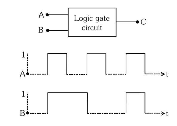
The following figure showns a AND logic gate circuit with two inputs A and B and the output C. The voltage waveforms at C will be -
View SolutionThe following figure shows a logic gate circuit with two inputs A and B and the output C. The voltage waveforms of A, B and C are as shown below.
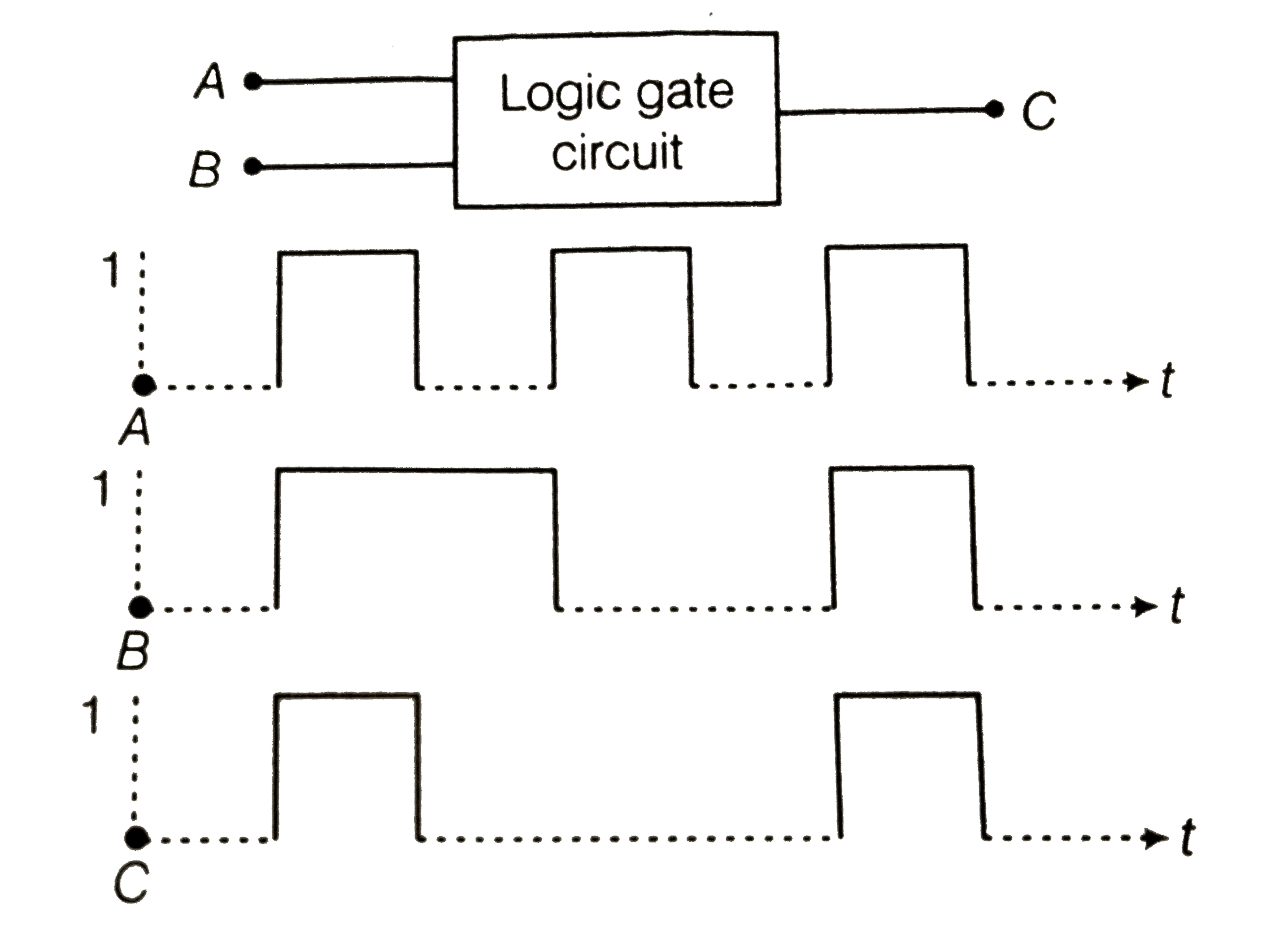
The logic circuit gate is
View Solution
Knowledge Check
The following figure shows a logic gate circuit with two inputs A and B and the output C. The voltage waveforms of A,B and C are as shown below
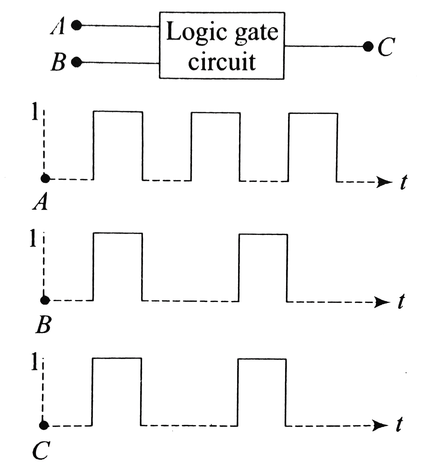 AAND gateBNAND gateCNOR gateDOR gate
The following figure shows a logic gate circuit with two inputs A and B and the output Y. The voltage waveforms of A,B and Y are as given :
The logic gate isANOR gateBOR gateCAND gateDNAND gateThe following figure shows a logic gate circuit with two inputs A and B and the output Y. The voltage waveforms of A,B and the output Y are as given
 ANOR gateBOR gateCAND gateDNAND gate
The following figure shows a logic gate circuit with two inputs A and B and the output C. The voltage waveforms of A, B and C are as shown below-
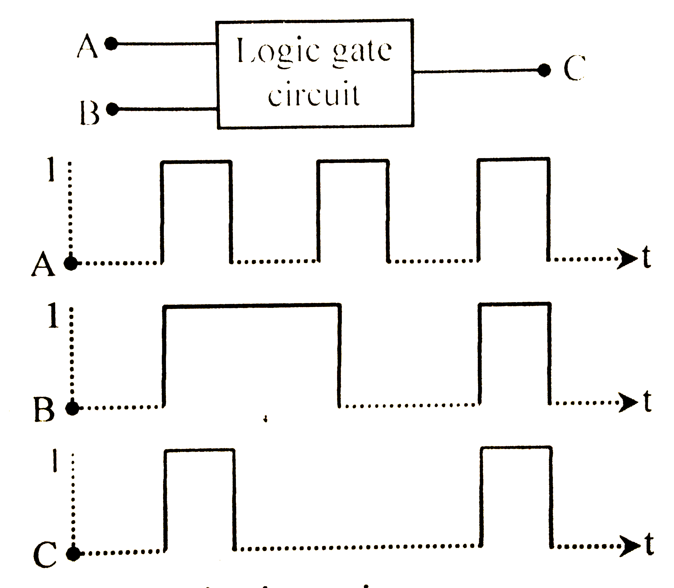
View SolutionThe following figure shows a logic gate circuit with two inputs A and B and the output C. The voltage waveforms of A, B and C are as shown below
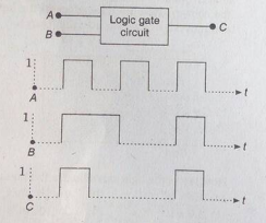
The logic circuit gate is
View SolutionThe following figure shows a logic gate circuit with two inputs A and B and the output C. The voltage waveforms of A, B and C are as shown below

The logic circuit gate is
View SolutionThe following figure shows a logic gate circuit with two inputs A and B output C. The voltage waveforms of A,B and C are as shown in second figure given below :-
_E01_436_Q01.png)
The logic circuit gate is :-
View SolutionThe following shows a logic gate circuit with two inputs A and B and the output C. The voltage waveforms of A, B and C are as shown below.
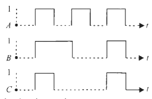
The logic circuit gate is
View Solution
