Transistor input characteristics curves are the graphs drawn with
Collector current IC on y-axis and the collector emitter voltage VCE on X-axis for a constant base current
Base current IB on y-axis and the base-emitter voltage VBE on X-axis for a constant collector emitter voltage
Base current IB on y-axis and the collector emitter voltage (VCB) on x-axis for a constant collector current
Base current IB on y-axis and collector current IC on x-axis with constant base emitter voltage
The correct Answer is:B
To solve the question regarding the transistor input characteristics curves, we need to analyze the options provided and determine which one correctly describes the input characteristics of a transistor.
1. Understanding Input Characteristics:
- The input characteristics of a transistor refer to the relationship between the base current (IB) and the base-emitter voltage (VBE) while keeping the collector-emitter voltage (VCE) constant.
2. Analyzing the Options:
- Option 1: Collector current (IC) on y-axis and collector-emitter voltage (VCE) on x-axis for a constant base current.
- This describes output characteristics, not input characteristics.
- Option 2: Base current (IB) on y-axis and base-emitter voltage (VBE) on x-axis for a constant collector-emitter voltage (VCE).
- This matches the definition of input characteristics.
- Option 3: Base current (IB) on y-axis and collector-emitter voltage (VCE) on x-axis for a constant collector current (IC).
- This does not represent input characteristics.
- Option 4: Base current (IB) on y-axis and collector current (IC) on x-axis with constant base-emitter voltage (VBE).
- This is also not an input characteristic.
3. Identifying the Correct Answer:
- From the analysis, Option 2 is the correct answer as it correctly describes the input characteristics of a transistor.
Final Answer:
Transistor input characteristics curves are the graphs drawn with base current (IB) on the y-axis and base-emitter voltage (VBE) on the x-axis for a constant collector-emitter voltage (VCE). Therefore, the correct option is Option 2.
- The input characteristics of a transistor refer to the relationship between the base current (IB) and the base-emitter voltage (VBE) while keeping the collector-emitter voltage (VCE) constant.
- Option 1: Collector current (IC) on y-axis and collector-emitter voltage (VCE) on x-axis for a constant base current.
- This describes output characteristics, not input characteristics.
- Option 2: Base current (IB) on y-axis and base-emitter voltage (VBE) on x-axis for a constant collector-emitter voltage (VCE).
- This matches the definition of input characteristics.
- Option 3: Base current (IB) on y-axis and collector-emitter voltage (VCE) on x-axis for a constant collector current (IC).
- This does not represent input characteristics.
- Option 4: Base current (IB) on y-axis and collector current (IC) on x-axis with constant base-emitter voltage (VBE).
- This is also not an input characteristic.
- From the analysis, Option 2 is the correct answer as it correctly describes the input characteristics of a transistor.
Transistor input characteristics curves are the graphs drawn with base current (IB) on the y-axis and base-emitter voltage (VBE) on the x-axis for a constant collector-emitter voltage (VCE). Therefore, the correct option is Option 2.
Topper's Solved these Questions
- BOOK - AAKASH SERIESCHAPTER - SEMICONDUCTOR DEVICESEXERCISE - EXERCISE -I (LOGIC GATES)17videos
SEMICONDUCTOR DEVICES
- BOOK - AAKASH SERIESCHAPTER - SEMICONDUCTOR DEVICESEXERCISE - EXERCISE -I (MATCHING TYPE QUESTIONS)9videos
SEMICONDUCTOR DEVICES
- BOOK - AAKASH SERIESCHAPTER - SEMICONDUCTOR DEVICESEXERCISE - EXERCISE -I (P-N JUNCTION DIODE)30videos
SEMICONDUCTOR DEVICES
- BOOK - AAKASH SERIESCHAPTER - RAY OPTICSEXERCISE - PROBLEMS ( LEVEL-II)60videos
RAY OPTICS
- BOOK - AAKASH SERIESCHAPTER - UNITS AND MEASUREMENTEXERCISE - PRACTICE EXERCISE45videos
UNITS AND MEASUREMENT
Similar Questions
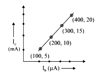
The transfer characteristic curve of a transistor, having input and output resistance 100Ωand100kΩ respectively, is shown in the figure. The Voltage and Power gain, are respectively:
 View Solution
The transfer characteristic curve of a transistor, having input and output resistance 100Ωand100kΩ respectively, is shown in the figure. The Voltage and Power gain, are respectively:
 View Solution
Knowledge Check
- Question 1 - Select One
The transfer characteristics of a base biased transistor has the operation regions, namely, cutoff, active region and saturation region. For using the transistor as an amplifier it has to operate in the
Aactive regionBcutoff regionCsaturation regionDcutoff and saturation - Question 2 - Select One
If y=3x2+6x+2 is graphed in the xy-plane, which of the following characteristics of the graph is displayed as a constant or coefficient in the equation?
Ay-coordinate of the vertexBx-intercept(s)Cy-interceptDx-intercept of the line of symmetry - Question 3 - Select One
The transfer ratio of a transistor is 50. The input resistance of the transistor when used in the common -emitter configuration is 1kΩ. The peak value for an A.C. input voltage of 0.01V peak is
A100μAB0.01μAC0.25μAD500μA
For a transistor in a common emitter mode, draw labelled graph to show :
(1) Input characteristic curve.
(2) Output characteristic curve.
(3) Transfer characteristic curve.
(Circuit diagram of the arrangement is not required.)View SolutionDraw the tramsfer characteristic curve of a base biased transistor in CE configuration. Explain clearly how the active region of the Vo versus Vi curve in a transistor is used as an amplifier.
View Solution(i) Draw a circuit diagram to study the input and output characteristics of an n-p-n transistor in its common emitter configuration. Draw the typical input and output characteristics.
(ii) Explain, with the hepl of a circuit diagram, the working of n-p-n transistor as a common emitter amplifier.View SolutionA realistic graph depiciting the variation of thhe reciprocal of input resistance in an in- put charcteristics measurement in a com- mon emitter transistor configuration is :
View SolutionThe transfer ratio of a transistor is 50. The input resistance of the transistor when used in the common -emitter configuration is 1kΩ. The peak value for an A.C. input voltage of 0.01V peak is
View Solution

