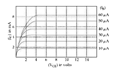
Transistor output characteristic curves are the graphs drawn with
Collector current IC on y-axis and the collector emitter voltageVCE on X-axis for a constant base current
Base current IB on y-axis and the base -emitter voltage VBE on x-axis for a constant collector emitter voltage
Base current IB on y-axis and the collector emitter voltage VCE on X-axis for a constant collector current
Base current IBon y-axis and collector current IC on X-axis with constant base - emitter voltage
The correct Answer is:A
To solve the question regarding the transistor output characteristic curves, we need to understand the definitions and relationships involved in the characteristics of a transistor. Let's break down the solution step by step.
1. Understanding Transistor Output Characteristics:
- Transistor output characteristics are graphical representations that show how the collector current (I_C) varies with the collector-emitter voltage (V_CE) for different values of base current (I_B).
2. Identifying the Axes:
- In these characteristic curves, the Y-axis typically represents the collector current (I_C), while the X-axis represents the collector-emitter voltage (V_CE).
3. Constant Parameter:
- The curves are plotted for constant values of the base current (I_B). This means that for each curve on the graph, the base current is held constant while varying the collector-emitter voltage (V_CE) to observe the changes in collector current (I_C).
4. Analyzing the Options:
- Option 1: Collector current (I_C) on Y-axis and collector-emitter voltage (V_CE) on X-axis for a constant base current.
- Option 2: Base current (I_B) on Y-axis and base-emitter voltage (V_BE) on X-axis for a constant collector-emitter voltage.
- Option 3: Base current (I_B) on Y-axis, collector-emitter voltage (V_CE) on X-axis for a constant collector current.
- Option 4: Base current (I_B) on Y-axis and collector current (I_C) on X-axis with constant base-emitter voltage.
5. Selecting the Correct Option:
- Based on the definitions and the analysis above, the correct representation for the transistor output characteristic curves is Option 1: Collector current (I_C) on Y-axis and collector-emitter voltage (V_CE) on X-axis for a constant base current.
Final Answer:
The correct answer is Option 1: Collector current (I_C) on Y-axis and collector-emitter voltage (V_CE) on X-axis for a constant base current.
---
- Transistor output characteristics are graphical representations that show how the collector current (I_C) varies with the collector-emitter voltage (V_CE) for different values of base current (I_B).
- In these characteristic curves, the Y-axis typically represents the collector current (I_C), while the X-axis represents the collector-emitter voltage (V_CE).
- The curves are plotted for constant values of the base current (I_B). This means that for each curve on the graph, the base current is held constant while varying the collector-emitter voltage (V_CE) to observe the changes in collector current (I_C).
- Option 1: Collector current (I_C) on Y-axis and collector-emitter voltage (V_CE) on X-axis for a constant base current.
- Option 2: Base current (I_B) on Y-axis and base-emitter voltage (V_BE) on X-axis for a constant collector-emitter voltage.
- Option 3: Base current (I_B) on Y-axis, collector-emitter voltage (V_CE) on X-axis for a constant collector current.
- Option 4: Base current (I_B) on Y-axis and collector current (I_C) on X-axis with constant base-emitter voltage.
- Based on the definitions and the analysis above, the correct representation for the transistor output characteristic curves is Option 1: Collector current (I_C) on Y-axis and collector-emitter voltage (V_CE) on X-axis for a constant base current.
The correct answer is Option 1: Collector current (I_C) on Y-axis and collector-emitter voltage (V_CE) on X-axis for a constant base current.
Topper's Solved these Questions
- SEMICONDUCTOR DEVICESBOOK - AAKASH SERIESCHAPTER - SEMICONDUCTOR DEVICESEXERCISE - EXERCISE -I (LOGIC GATES)
17 Videos
- SEMICONDUCTOR DEVICESBOOK - AAKASH SERIESCHAPTER - SEMICONDUCTOR DEVICESEXERCISE - EXERCISE -I (MATCHING TYPE QUESTIONS)
9 Videos
- SEMICONDUCTOR DEVICESBOOK - AAKASH SERIESCHAPTER - SEMICONDUCTOR DEVICESEXERCISE - EXERCISE -I (P-N JUNCTION DIODE)
30 Videos
- RAY OPTICSBOOK - AAKASH SERIESCHAPTER - RAY OPTICSEXERCISE - PROBLEMS ( LEVEL-II)
60 Videos
- UNITS AND MEASUREMENTBOOK - AAKASH SERIESCHAPTER - UNITS AND MEASUREMENTEXERCISE - PRACTICE EXERCISE
45 Videos
Similar Questions
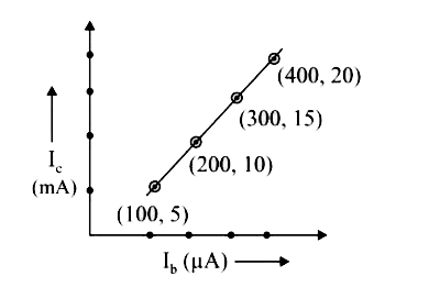
The transfer characteristic curve of a transistor, having input and output resistance 100Ωand100kΩ respectively, is shown in the figure. The Voltage and Power gain, are respectively:

View SolutionThe transfer characteristic curve of a transistor, having input and output resistance 100Ωand100kΩ respectively, is shown in the figure. The Voltage and Power gain, are respectively:

View SolutionA certain n-p-n transistor has the common emitter output characteristics as shown in the figure.
(a) Find the emitter current at VCE=12.5VandIb=60μA,and
(b) Current gain 'β' at this point.
View SolutionFor a transistor in a common emitter mode, draw labelled graph to show :
(1) Input characteristic curve.
(2) Output characteristic curve.
(3) Transfer characteristic curve.
(Circuit diagram of the arrangement is not required.)
View SolutionDraw the tramsfer characteristic curve of a base biased transistor in CE configuration. Explain clearly how the active region of the Vo versus Vi curve in a transistor is used as an amplifier.
View SolutionThe output characteristics of a transistor is shown in the figure. When VCE is 10 V and IC=4.0mA, then value of βac is _________

View SolutionConsider an amplifier circuit using a transistor.The output power is several times greater than the input power.Where does the extra power come from?
View SolutionConsider an amplifier circuit using a transistor.The output power is several times greater than the input power.Where does the extra power come from?
View SolutionDraw the diagram of the circuit arangement used for studying the 'input' and the 'output' characteristics of an n-p-n transistor inits CE configuration. Briefly explain how these two types of characteristics are obtained and draw these characteristics.
(b) 'Define' the terms (i) Input resistance, (ii) Output resistance , (iii) Current amplification factor, for a given transistor.
View Solution(i) Draw a circuit diagram to study the input and output characteristics of an n-p-n transistor in its common emitter configuration. Draw the typical input and output characteristics.
(ii) Explain, with the hepl of a circuit diagram, the working of n-p-n transistor as a common emitter amplifier.
View Solution
