Complete Solutions to Assignment section -A (Objective Type Question) of chapter SEMICONDUCTOR ELECTRONICS (MATERIAL, DEVICES AND SIMPLE CIRUITS ) of Class 12 book with complete answers and questions
| Class 12 | PHYSICS |
| Chapter | SEMICONDUCTOR ELECTRONICS (MATERIAL, DEVICES AND SIMPLE CIRUITS ) |
| AAKASH INSTITUTE | Assignment section -A (Objective Type Question) |
| Number Of Questions | 43 |
| Academic Year | 2023-24 |
The semiconductor are generally
View SolutionThe conductivity of a semiconductor depends upon
View SolutionThe impurity atoms with which pure silicon should be doped to make a p- type semiconductor are those of
View SolutionIn semiconductors, which one of the following relations is correct at thermal equilibrium?
View SolutionIn a semiconductor,
View SolutionThe rate of recombination or generation are governed by the law(s) of
View SolutionAn n-type semi- conductor is
View SolutionSolids having highest energy level partially filled with electrons are
View SolutionThe energy gap for an insulator may be
View SolutionIf `N_(A)` is number density of acceptor atoms added and `N_(D)` is number density of donor atoms added to a semiconductor, `n_(e) and n_(h)` are the number density of electrons and holes in it, then
View SolutionIn an unbiased p-n junction which of the following is correct?
View SolutionWith an ac input from 50 Hz power line, the ripple frequency is
View SolutionIn a semiconductor diode, reserve bias current is due to drift of free electrons and holes caused by
View SolutionThe value of form factor in case of half wave rectifier is
View SolutionIn a semiconductor diode p-side is earthed and N-side is applied a potential of -2V, the diode shall
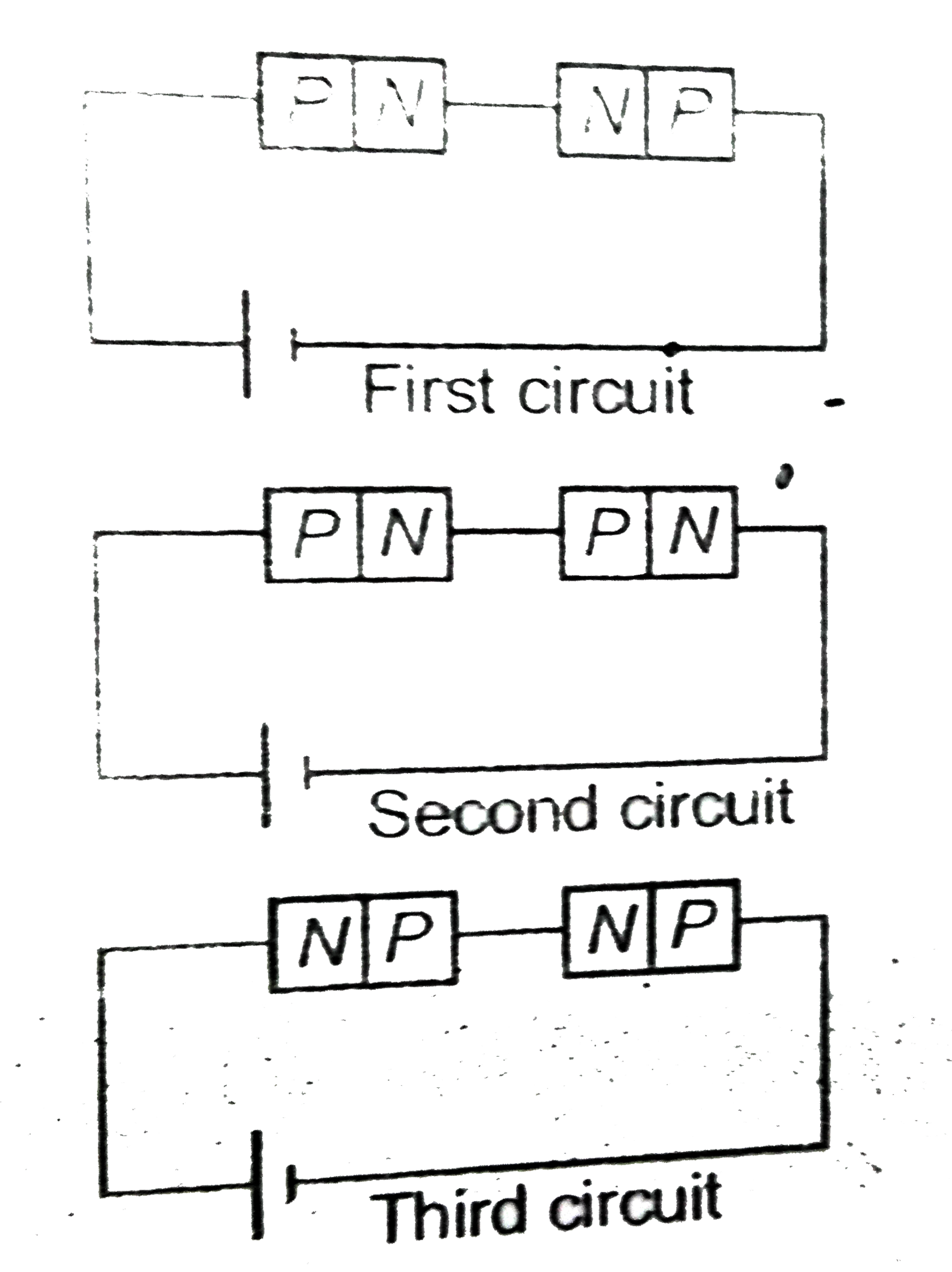
View SolutionTwo identical P-N junctions, may be connected in series with a battery in three ways as shown in the adjoining fiugre. The potential drop across the P-N junction are equals in

View SolutionZener diode is used for:-
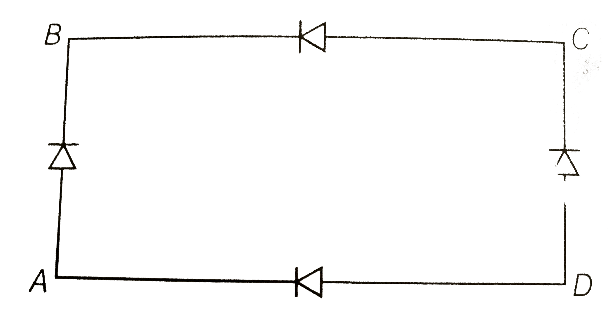
View SolutionIn figure the input is across the terminals A and C and the output is across B and D. Then the output is

View SolutionA junction diode , in which one of the p or n - sections is made very thin, can be used to convert light energy into electrical energy, then the diode is called
View SolutionThe materials suitable for making a solar cell is
View SolutionIn which of the configuration of a transistor , the power gain is highest ?
View SolutionIn a common base amplifier the phase difference the input signal voltage and the output voltage is
View SolutionThe current transfer ratio `beta` of a transistor is 100. The input resistance of the transistor when used in common emitter mode is 1 kilo ohm. The peak value of the collector alternating current for an input peak voltage of 0.01 volt is
View SolutionIn a common emitter transistor circuit, the base current is `40 muA` , then `V_(BE)` is
View SolutionThe emitter region in a PNP-junction transistor is more heavily doped than the base region, so that
View SolutionA transsitor is operated in CE configuration at `V_(CC) = 2 V` such that a change in base current from 100 `muA` to 200 `muA` produces a change in the collector current from 9mA to 16.5 mA. The value of current gain, `beta` is -
View SolutionThe input resistance of a silicon transistor is `665Omega`. Its base current is changed by `15muA` which results in the change in collector current by `2mA`. This transistor is used as a common emitter amplifier with a load resistance of `5kOmega`. What is the voltage gain of the amplifier.
View SolutionThe relationship between `alpha` and `beta` is given by
View SolutionIn a common base transistor circuit, the current gain is 0.98. On changing the emitter current by 1 mA, the change in collector current is
View SolutionFor a transistor amplifier power gain and voltage gain are `7.5 and 2.5` respectively. The value of the current gain will be
View SolutionThe input resistance of a common-emitter amplifier is `2 kOmega` and a.c. Current gain is 20. If the load resistance used is `5 kOmega`, calculate the transconductance of the transistor used
View SolutionIn a silicon transistor, a change of `7.89 mA` in the emitter current produce a change of 7.6 mA in the collector current. What change in the base current is necessary to produce an equivalent change in the collector current?
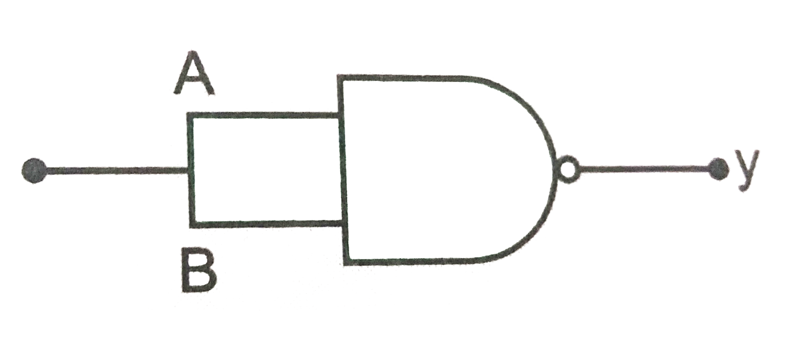
View SolutionThe abjoining logic symbol is equivalent to

View SolutionWhich of the following gates corresponds to the truth table given below?

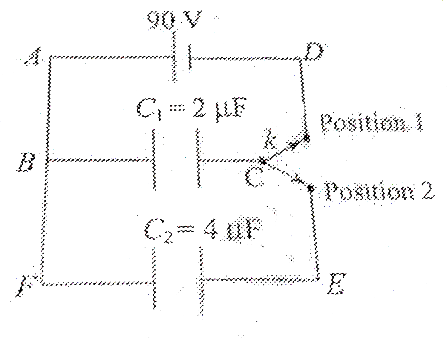
View SolutionFigure shows two capacitors of capacitance `2muF` and `4muF` and a cell of 90 V. The switch 'k' is such that when it is in position 1, the circuit ABCD is closed and when it is in position 2, the circuit BCEF is closed.the resistance of both the circuits is negligible os that the capacitor gets fully charged instantly. Initially the switch is in position1. then it is turned in position 2 and then in position 1. Now two cycles are completed. Find the charge `("in" mu C)` after two cycles.

View SolutionThe combination of gates shown in the circuit is equivalent to

View SolutionFind Y

View SolutionWrite down the boolean experssion for output Y of a system shown in figure

View SolutionCopper has face-centered cubic (fcc) lattice with interatomic spacing equal to `2.54 Å`. The value of lattice constant for this lattice is
View SolutionIf a is the length of the side of a cube, the distance between the body centered atom and one corner atom in the cube will be.
View SolutionLiquid crystal display monitors are made of
View SolutionWhich of the following cannot be obtained from an IC?
View SolutionOperational amplifier is a
View Solution
Assignment section -A (Objective Type Question) questions and complete solutions for chapter SEMICONDUCTOR ELECTRONICS (MATERIAL, DEVICES AND SIMPLE CIRUITS ) of AAKASH INSTITUTE ENGLISH of Class 12