Complete Solutions to TRY YOUR SELF of chapter SEMICONDUCTOR ELECTRONICS (MATERIAL, DEVICES AND SIMPLE CIRUITS ) of Class 12 book with complete answers and questions
| Class 12 | PHYSICS |
| Chapter | SEMICONDUCTOR ELECTRONICS (MATERIAL, DEVICES AND SIMPLE CIRUITS ) |
| AAKASH INSTITUTE | TRY YOUR SELF |
| Number Of Questions | 27 |
| Academic Year | 2023-24 |
In semiconductors at a room temperature
View SolutionCarbon, silicon and germanium have four valence electrons each. These are characterised by valence and conduction bands separated by energy band gap respectively equal to `(E_g)_C, (E_g)_(Si), and (E_g)_(Ge)`. Which of the following statements is true?
View SolutionIn a pure semiconductor, the number of conduction electron is `6xx10^(19)` per cubic meter. How many holes are there in a sample of size 1 cm x 2 cm x 2mm ?
View SolutionC, Si and Ge have same lattice structure. Why is C insulator while Si and Ge intrinsic semiconductors?
View SolutionA semiconductor is known to have an electron concentration of `6xx10^(12)` per cubic centimeter and a hole concentration of `9xx10^(13)` per cubic centimeter. Is this semiconductor N-type or P-type ?
View SolutionSuppose a pure Si-crystal has `6xx10^(28) "atoms" m^(-3)`. It is doped by 1 ppm concentration of pentavalent As. Calculate the number of electrons and holes. Give that `n_(i)=1.5xx10^(16)m^(-3)`.
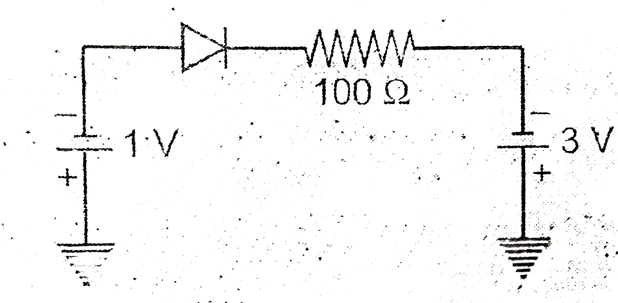
View SolutionWhat is the current through an ideal p-n junction diode shown in figure below ?

View SolutionIf in p-n junction diode a sinusoidal input signal is applied as shown Then the output signal across `R_(L)` will bw
View SolutionIn a reverse biased diode, when the applied voltage changes by `1V`, the current is found to change by `0.5muA`. The reversebiase resistance of the diode is
View SolutionPotential drop across forward junction p-n diode is `0.7` V. If a battery of 4 V is applied, calculate the resistance to be put in series, if the maximum current in the circuit is `5 mA`.
Hint: `R = 4 - 07/5 xx 10^(-3) = 660 Omega`
View SolutionPotential barrier developed in a junction diode opposes the flow of
View SolutionA forward biased diode is
View SolutionApplication of forward bias to p-n junction
View SolutionIn a p-n junction having depletion layer of thickness `10^(-6)` m the potential across it is `0.3 V`. Then the electric field is
Hint = `E= V/d`
View SolutionPickout the incorrect statement regarding reverse saturation current in the `p-n` junction diode.
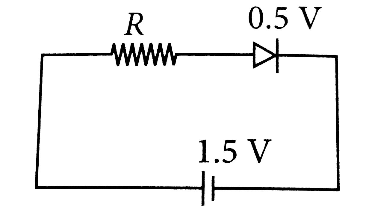
View SolutionThe diode used in the circuit shown in the figure has a constant voltage drop at 0.5 V at all currents and a maximum power rating of 100 mW. What should be the value of the resistor R, connected in series with diode, for obtaining maximum current ?

View SolutionWith an ac input from 50 Hz power line, the ripple frequency is
View SolutionFreuency of given AC signal is 50 Hz. When it connected to a half - wave rectifier, then what is the number of output pulses given by rectifier within one second ?
View SolutionWhat is the output form of full-wave rectifier ?
View SolutionIn a Zener regulated power supply a Zener diode with `V_(Z) = 6.0` V is used for regulation. The load current is to be 4.0 mA and the unregulated input is 10.0 V. What should be the value of series resistor `R_(S)`?
View SolutionThe current in the forward bias is known to be more (-mA) than the current in the reverse bias `(-mu A)`. What is the reason, then, to operate the photodiode in reverse bias ?
View SolutionWhy are Si and GaAs are preferred materials for solar cells?
View SolutionFor a CE transistor amplifier , the audio signal voltage across the collector resistance of `2K Omega` is 2V. Suppose the current amplification factor of the transistor is 100. what should be the value of `R_(B)` in series with `V_(BB)` supply of 2V if the dc base current has to be 10 times the signal current. Also calculate the dc drop across the collector resistance. (Refer to figure of CE amplifier) . Take `V_(BE)=0.6V`
View SolutionIn the figure of transistor as a switch, the `V_(BB)` supply can be varied from 0V to 5V. The Si transistor has `beta_(dc)=250` and `R_(B)=100 kOmega,R_(C)=1 kOmega,V_(C C)=5V`. Assume that when the transistor is saturated, `V_(CE)=0V` and `V_(BE)=0.8V` . calculate
(a) the minimum base current for which the transistor will reach saturation. hence.
(b) Determine `V_(i)` when the transistor is switched on
(C) Find the ranges of `V_(i)` for which the transistor is switched off and switched on'
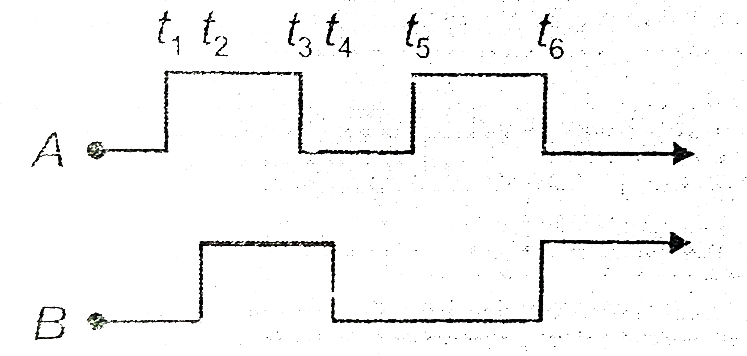
View SolutionShow the output waveform of OR gate for the following input waveforms of A and B

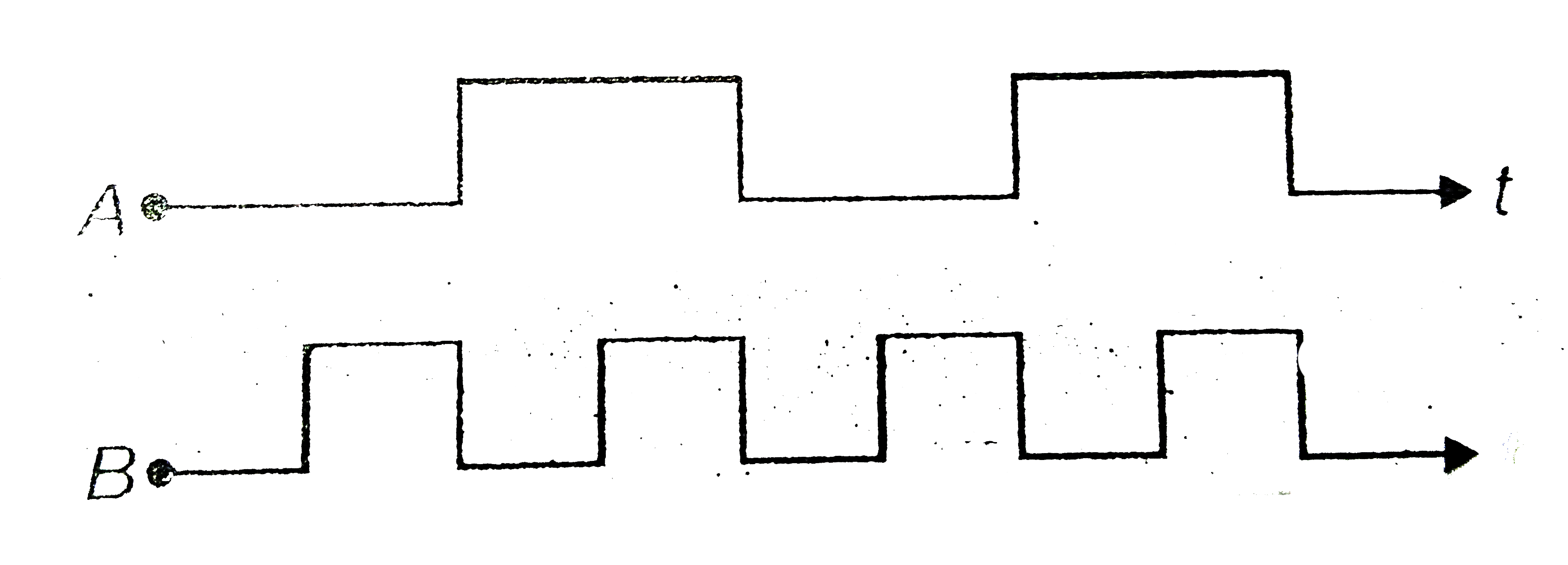
View SolutionSketch the output waveform obtained from AND gate for the following inputs A and B.

View SolutionSketch the output waveform Y from a NAND gate having following inputs A and B

View Solution
TRY YOUR SELF questions and complete solutions for chapter SEMICONDUCTOR ELECTRONICS (MATERIAL, DEVICES AND SIMPLE CIRUITS ) of AAKASH INSTITUTE ENGLISH of Class 12