Complete Solutions to Assignment section -C (Previous years type question) of chapter SEMICONDUCTOR ELECTRONICS (MATERIAL, DEVICES AND SIMPLE CIRUITS ) of Class 12 book with complete answers and questions
| Class 12 | PHYSICS |
| Chapter | SEMICONDUCTOR ELECTRONICS (MATERIAL, DEVICES AND SIMPLE CIRUITS ) |
| AAKASH INSTITUTE | Assignment section -C (Previous years type question) |
| Number Of Questions | 100 |
| Academic Year | 2023-24 |
Which of the following represents forward biase diode?
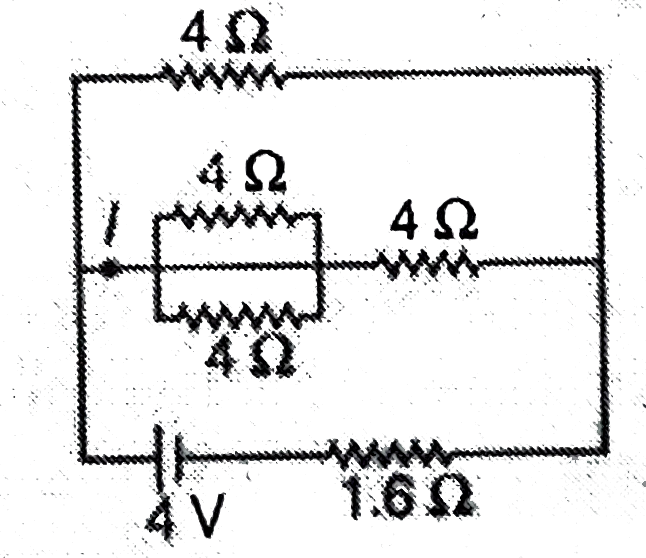
View SolutionThe given electrical network is equivalent to
View SolutionIn a common emitter transistor amplifier the audio signal voltage across the collector is `3 V`. The resistance of collector is `3 kOmega`. If current gain is `100` and the base resistance is `2 kOmega`, the voltage and power gain of the amlifier is :
View SolutionFor CE transistor amplifier, the audio signal voltage across the collector resistance of `2 kOmega` is 4V. If the current amplification factor of the transistor is 100 and the base resistance is `1kOmega`, then the input signal voltage is
View SolutionThe given circuit has two ideal diodes connected as shown in the figure below. The current flowing through the resistance `R_(1)` will be
View SolutionWhat is the output Y in the following circuit, when all the three inputs A, B, C are first 0 and then 1?

View SolutionTo get output 1 for the following circuit, the correct choice for the input is

View SolutionConsider the junction diode as ideal. The value of current flowing through AB is

View SolutionA n-p-n transisitor is connected in common emitter configuration in a given amplifier. A load resistance of `800 Omega` is connected in the collector circuit and the voltage drop across it is `0.8 V`. If the current amplification factor is `0.96` and the input resistance of the circuits is `192 Omega`, the voltage gain and the power gain of the amplifier will respectively be
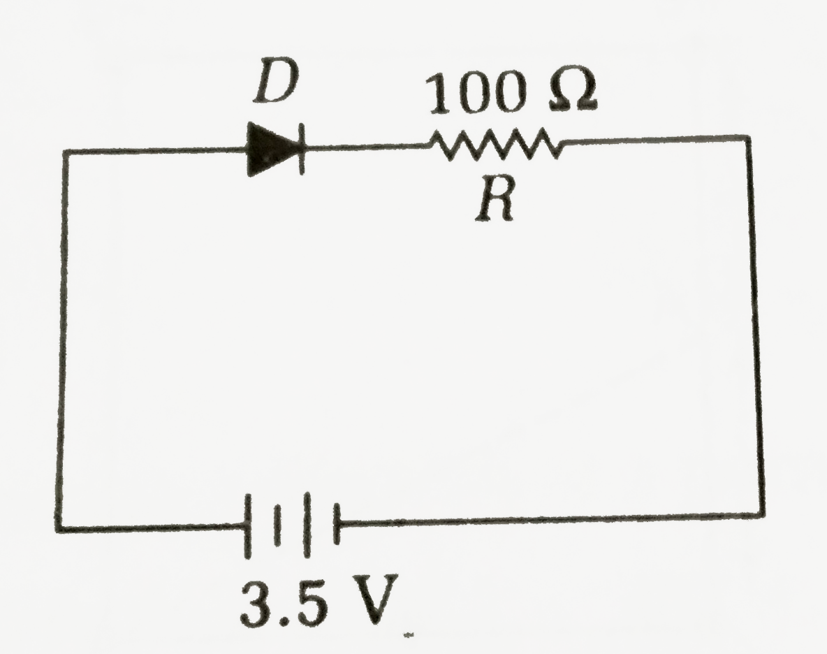
View SolutionIn the given figure, a dipole D is connected to an external resistance `R = 100 Omega` and an e.m.f. of `3.5 V`. If the barrier potential developed across the dipole is `0.5V`, the current in the circuit will be
View SolutionThe input signal given to a CE amplifier having a voltage gain of 150 is `V_(i) = 2 cos (15t + (pi)/(2))`. The corresponding output signal will be
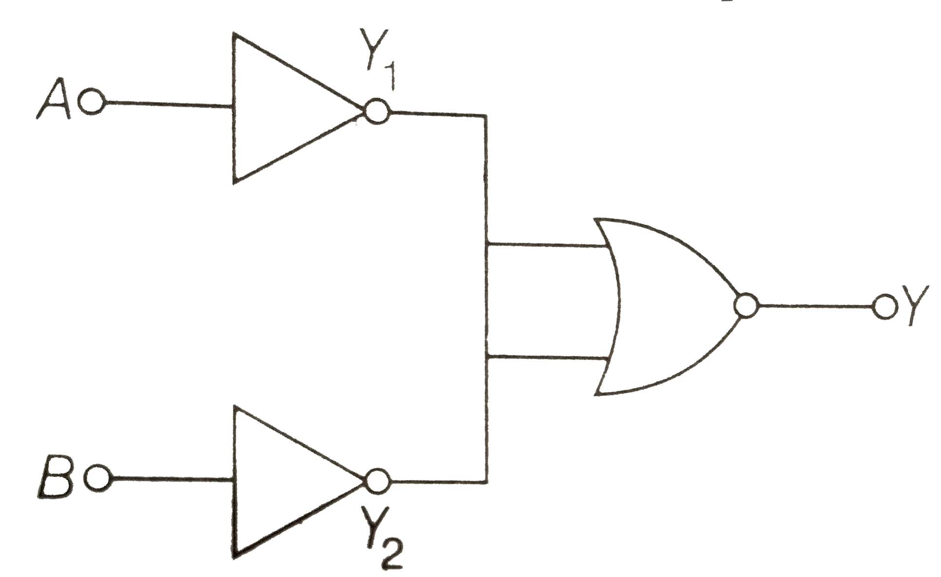
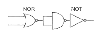
View SolutionWhich logic gate is represented by the following combination of logic gates?
View SolutionIf in a p-n junction, a square input signal of `10 V` is applied as shown,

then the output across `R_(L)` will be
View SolutionGiven
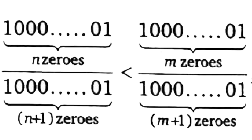
then which of the following true
View SolutionThe barrier potential of a p-n junction depends on
(i) type of semiconductor material
(ii) amount of doping
(iii) temperature
Which one of the following is correct ?
View SolutionIn a n-type semiconductor, which of the following statement is true ?
View SolutionIn a common emitter (CE) amplifier having a voltage gain G, the transistor used has transconductor 0.03 mho and current gain 25. If the above transistor is replaced with another one with transconductance 0.02 mho and current gain 20, the voltage gain will
View SolutionThe output (X) of the logic circuit shown in figure will be

View SolutionTwo ideal diodes are connected to a battery as shown in the circuit. The current supplied by the battery is
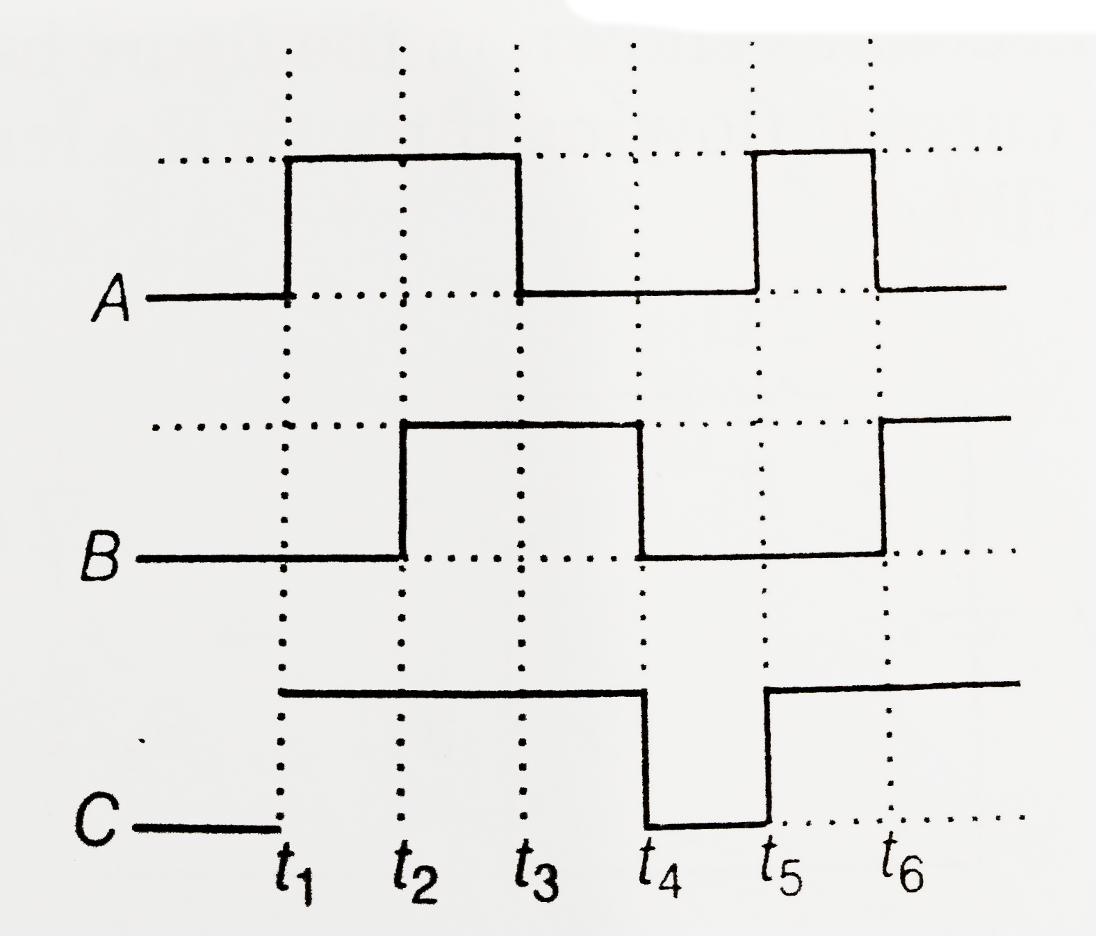
View SolutionThe figure shows a logic circuit with two inputs A and B and the output C. The voltage wave forms across A, B and C are as given. The logic circuit gate is
View SolutionIn a CE transistor amplifier, the audio signal voltage across the collector resistance of `2 kOmega` is 2V. If the base resistance is `1kOmega` and the current amplification of the transistor is 100, the input signal voltage is
View SolutionC and Si both have same lattice structure, having 4 bonding electrons in each. However, C is insulator whereas Si is intrinsic semiconductor. This is because
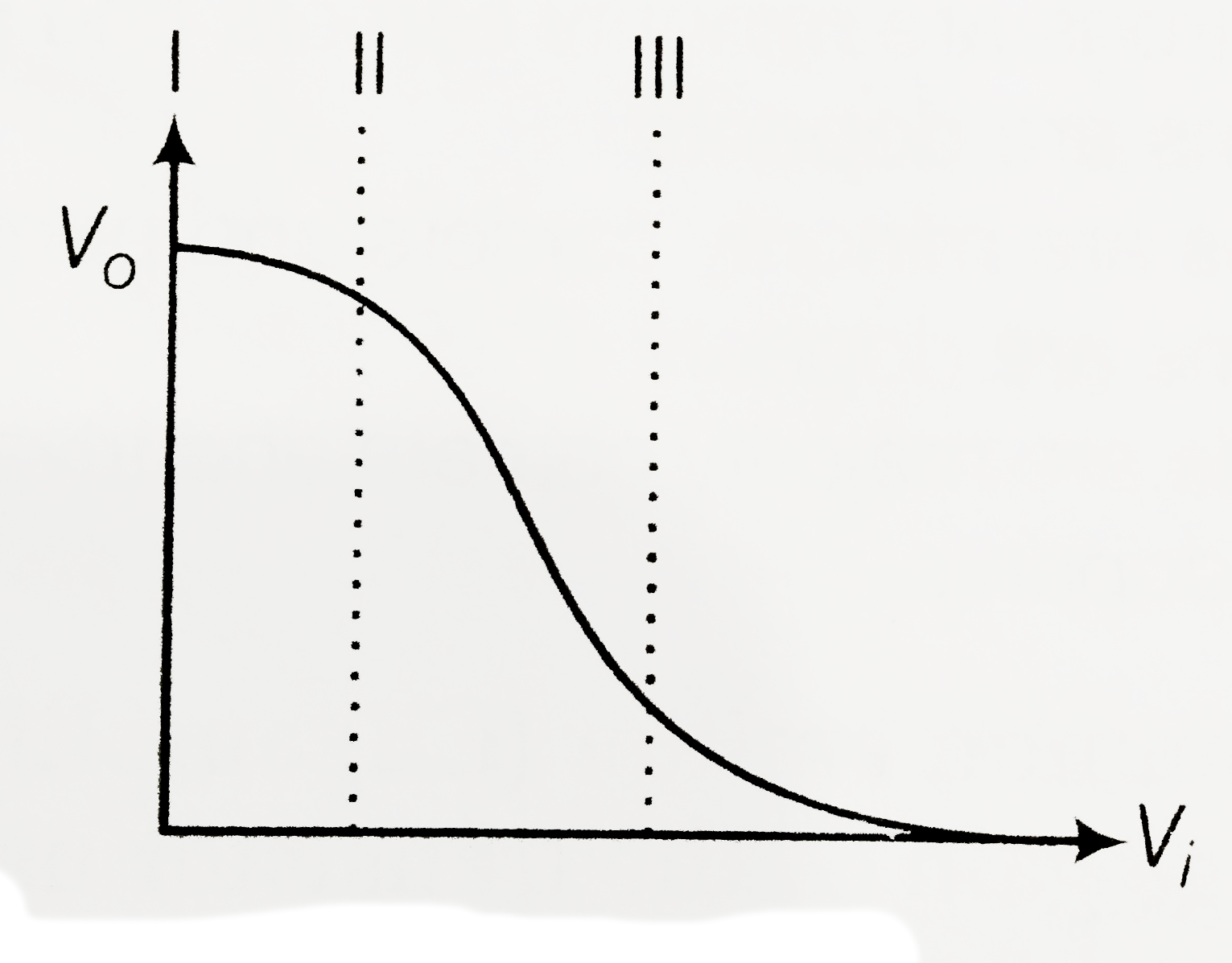
View SolutionTransfer characteristic [output voltage `(V_(0))` vs input voltage `(V_(i))` for a base biased transistor in CE configuration is as shown in the figure. For using transistor as a switch, it is used
View SolutionThe input resistance of a silicon transistor is `100 Omega`. Base current is changed by `40 muA` which results in a change in collector current by 2 mA. This transistor is used as a common emitter amplifier with a load resistance of `4 KOmega`. The voltage gain of the amplifier is-
View Solution
To get an output `Y=1` in given circuit which of the following input will be correct:
View SolutionA transistor is operated in common emitter configuration at `V_(c)=2 V` such that a change in the base current from `100 muA` to `300 muA` produces a change in the collector current from `10 mA` to `20 mA`. The current gain is
View SolutionIf a small amount of antimony is added to germanium crystal
View SolutionIn forward biasing of the p-n junction
View SolutionSymbolic representation of four logic gates are shown as
(i)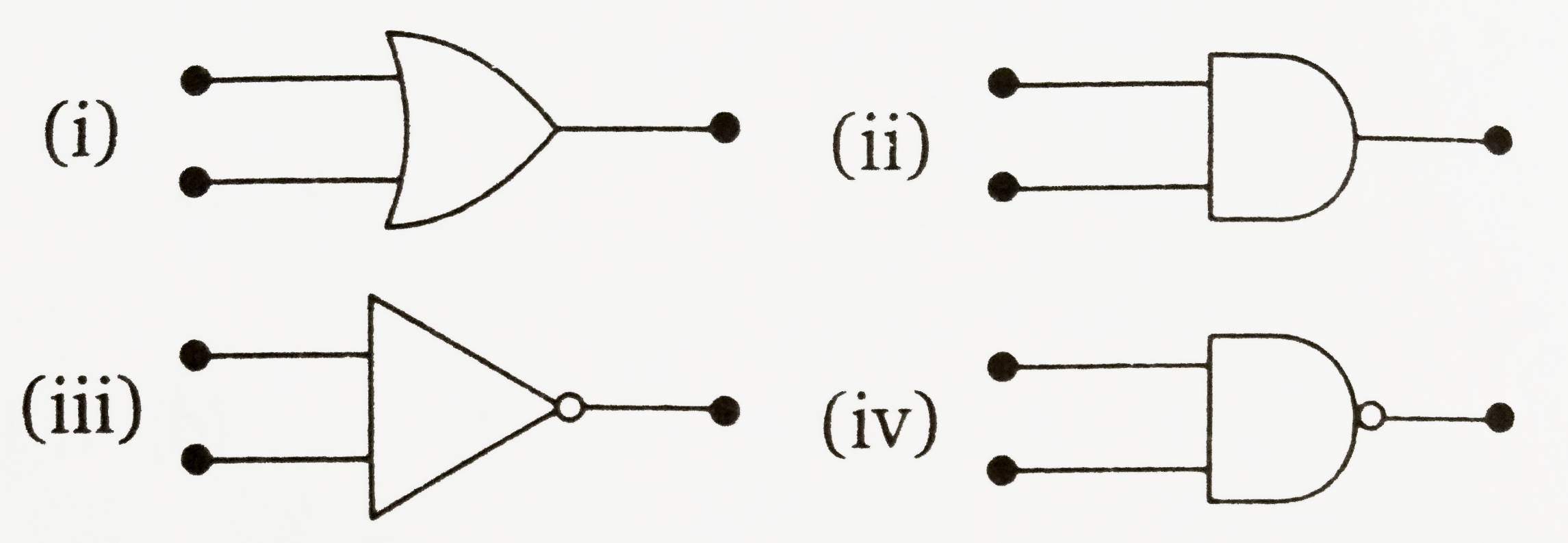
Pick out which ones are for AND, NAND and NOT gates, respectively.
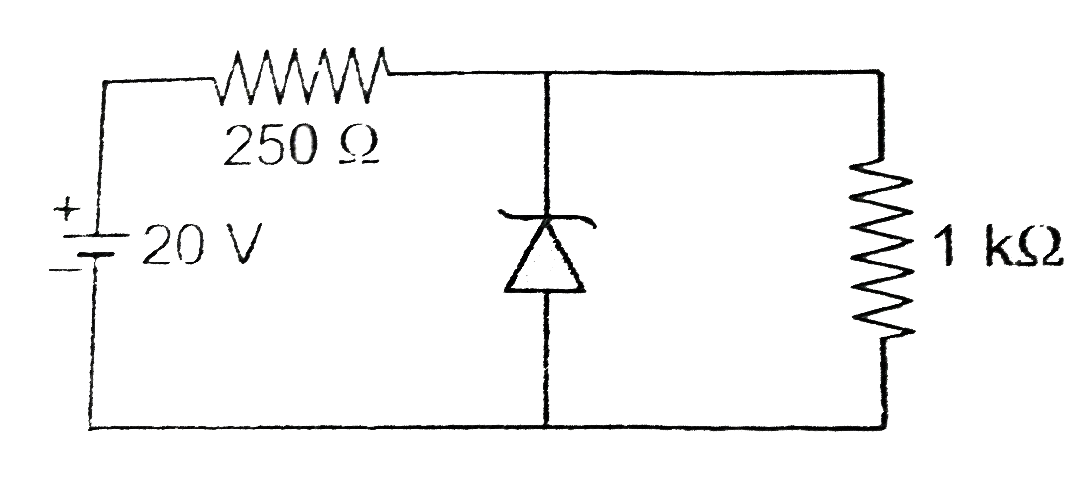
View SolutionA zener diode having breakdown voltage equal to 15V, is used in a voltage regulator circuit shown in figure. Find the current through the diode.
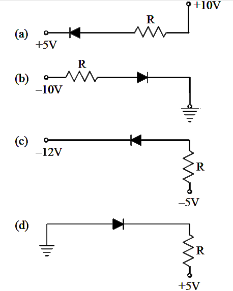
View SolutionIn the following figure, the diodes which are forwards biased are :
View SolutionPure Si at 500 K has equal number of electron `(n_(e))` and hole `(n_(h))` concentration of `1.5xx10^(16) m^(-3)`. Doping by indium increases `n_(h)` to `4.5xx10^(22) m^(-3)`. The doped semiconductor is of :
View SolutionA common emitter amplifier has a voltage gain of 50, an input impedance of `100 Omega` and an output impedance of `200 Omega`. The power gain the amplifier is
View SolutionTo get an output 1 from the circuit shown in figure the input must be :

View SolutionThe device that can act as a complete electronic circuit is
View SolutionWhich of the following statement is false?
View SolutionWhich one of the following bonds produces a solid that refleets light in the light in the visible region and whose electrical conductivity decreases with temperature and has high melting point ?
View SolutionThe following figure shows a logic gate circuit with two inputs A and B and the output C. The voltage waveforms of A, B and C are as shown below
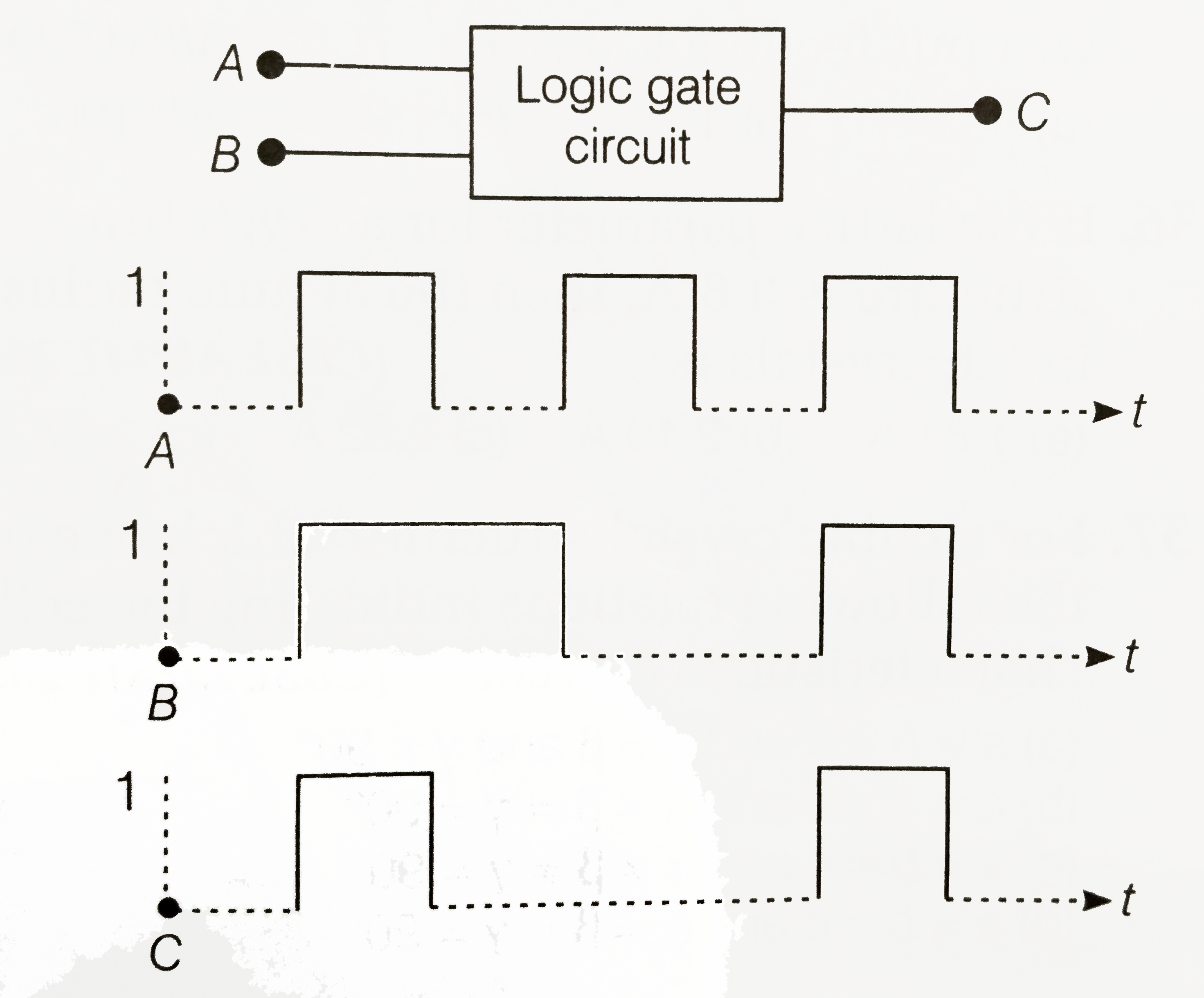


The logic circuit gate is
View SolutionThe vapour pressure of two pure liquids A and B that forms an ideal solution are 300 and 800 torr respectively at temperature T. A mixture of the vapours of A and B (for which the mole fraction of A is 0.25) is slowly compressed at temperature T. The vapour pressure of this condensate is meansured to be 'P'. What is the value of 684-P ?
View SolutionThe symbolic representation of four logic gates are given below :
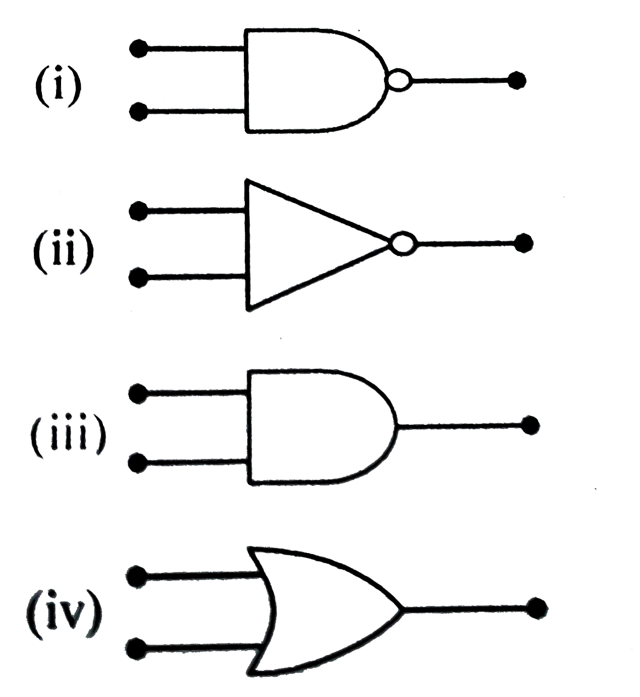
The logic symbols for OR, NOT and NAND gates are respectively :
View SolutionA p-n Photodiode is fabricated from a semiconductor with a band gap of 2.5 eV. The signal wavelength is
View SolutionA transistor is operated in common-emitter configuration at `V_(c) = 2` volt such that a change in the base current from `100 mu A` to `200 mu A` produces a change in the collector current from `5mA` to `10 mA`. The current gain is
View SolutionSodium has body centred packing. Distance between two nearest atoms is 3.7 Å. The lattice parameter is :
View SolutionIf the lattice parameter for a crystalline structure is `3.6Å`, then the atomic radius of fcc crystals is
View SolutionThe voltage gain of an amplifier with `9%` negative feedback is 10. The voltage gain without feedback will be
View SolutionThe circuit
View SolutionA p-n photodiode is made of a material with a band gap of `2.0 eV`. The minimum frequency of the radiation that can be absorbed by the material is nearly
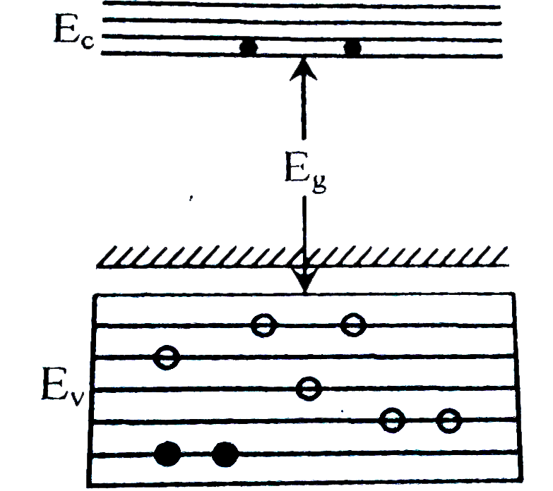
View SolutionIn the energy band diagram of a material shown below, the open circles and filled circles denote holes and electrons respectively. The material is:-
View SolutionA common emitter amplifier has a voltage gain of 50, an input impedance of `100 Omega` and an output impedance of `200 Omega`. The power gain the amplifier is
View SolutionIn the following circuit, the output Y for all possible inputs A and B is expressed by the truth table

View SolutionFor a cubic crystal structure which one of the following relation indicating the cell characteristic is correct ?
View SolutionA transistor is operated in common emitter configuration at constant collector voltage `V_(c) = 1.5V` such that a change in the base current from `100 mu A` to `150 mu A` produces a change in the collector current from `5mA` to `10 mA`. The current gain `(beta)` is
View SolutionA forward biased diode is
View SolutionThe following figure shows a logic gate circuit with two inputs A and B and the output C. The voltage waveforms of A, B and C are as given The logic circuit is:
View SolutionApplication of forward bias to p-n junction
View SolutionZener diode is used for:-
View SolutionCarbon, silicon and germanium have four valence electrons each. These are characterised by valence and conduction bands separated by energy band gap respectively equal to `(E_g)_C, (E_g)_(Si), and (E_g)_(Ge)`. Which of the following statements is true?
View SolutionChoose the false statement from the following.
View SolutionCopper has face-centered cubic (fcc) lattice with interatomic spacing equal to `2.54 Å`. The value of lattice constant for this lattice is
View SolutionThe cations and anions are arranged n alternate form in:
View SolutionIn semiconductors at a room temperature
View SolutionIn good conductors of electricity the type of bonding that exist is
View SolutionIn an insulator, the forbidden energy gap between the valence band and conduction band is of the order of
View SolutionIn a p-n junction depletion region has a thickness of the order of
View SolutionPure `Si` at 300 K has equal electron `(n_(e))` and hole `(n_(h))` concentrations of `1.5 xx 10^(18) m^(-3)`. Doping by indium increases `n_(h)` to `4.5 xx 10^(22) m^(-3)`. Calculate `n_(e)` in the dipoed `Si`.
View SolutionIn a reverse biased p-n junction, when the applied bias voltages is equal to the breakdown voltage, then
View SolutionIn the case of forward biasing of `PN`-junction, which one of the following figures correctly depicts the direction of flow of carriers?
View SolutionWhen arsenic is added as an impurity to silicon, the resulting material is
View SolutionTo obtain a p-type germanium semiconductor, it must be doped with
View SolutionThe cause of the potential barrier in a p-n diode is
View SolutionA semiconducting device is connected in a series in circuit with a battery and a resistance. A current is allowed to pass through the circuit. If the polarity of the battery is reversed, the current drops to almost zero. The device may be
View Solution`p-n` junction diode can be used as
View SolutionIn p-type semiconductor, the major charge carriers are:
View SolutionIn forward bias the width of depletion layer in a p-n junction diode
View SolutionDepletion layer consists of
View SolutionIn a junction diode, the holes are due to
View SolutionIn a PN junction : -
View SolutionFor the given circuit of P-N junction diode which is correct : -

View SolutionReverse bias applied to a junction diode
View SolutionBarrier potential of a p-n junction diode does not depend on -
View SolutionIn a p–n junction photo cell, the value of the photo electromotive force produced by monochromatic light is proportional to: -
View SolutionIn a zener diode, break down occurs in reverse bias due to
View SolutionIn a p-n junction, depletion region contains
View SolutionIn the given circuit , the value of current is
View SolutionThe diode used in the circuit shown in the figure has a constant voltage drop at 0.5 V at all currents and a maximum power rating of 100 mW. What should be the value of the resistor R, connected in series with diode, for obtaining maximum current ?
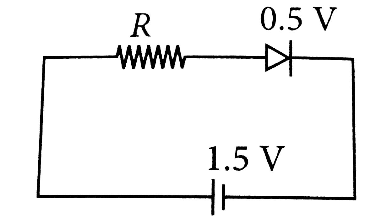
View SolutionThe current in the circuit will be
View SolutionIf a full wave rectifier circuit is operating from `50 Hz` mains, the fundamental frequency in the ripple frequency will be
View SolutionThe peak voltage in the output of a half wave diode rectifier fed with a sinusoidal signal without filter is 10V. The d. c. component of the output voltage is :-
View SolutionWhen a n-p-n transistor is used as an amplifier, then
View SolutionAn oscillator is nothing but an amplifier with
View SolutionThe correct relationship between the two current gains `alpha and beta` in a transistor is
View SolutionThe transfer ratio of a transistor is `50`. The input resistance of the transistor when used in the common -emitter configuration is `1 kOmega`. The peak value for an `A.C.` input voltage of `0.01 V` peak is
View SolutionFor a common emitter circuit if `l_(C)/l_(E) = 0.98` then current gain for common emtter circuit will be
View SolutionIn an n-p-n transistor working in active mode, the depletion region
View SolutionA transistor -oscillator using a resonant circuit with an inductor L (of negligible resistance) and a capacitor C in series produce oscillations of frequency f. If L is doubled and C is changed to 4 C, the frequency will be
View SolutionIn an n-p-n transistor working in active mode, the depletion region
View SolutionA transistor has a current amplification factor of 60. In a CE amplifier, input resistance is `1 kOmega` and output voltage is `0.01 V`. The transconductance is (in SI units)
View SolutionTo use a transistor as an amplifier
View SolutionIn a common emitter configuration base current is `40 mu A` and current gian is 100. The collector current will be
View SolutionWhich of the following gates correspond to the truth table given below ?
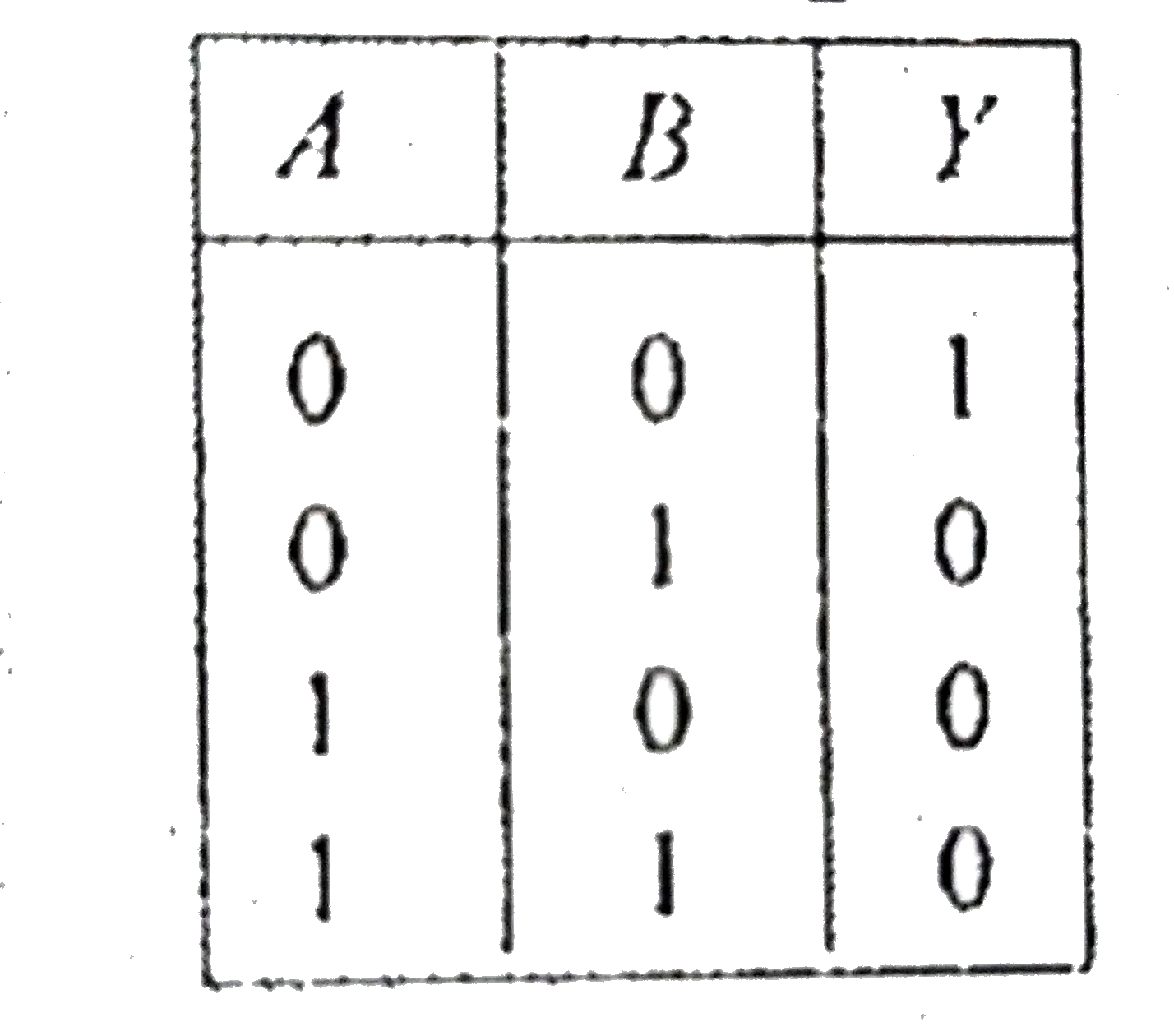
View Solution
Assignment section -C (Previous years type question) questions and complete solutions for chapter SEMICONDUCTOR ELECTRONICS (MATERIAL, DEVICES AND SIMPLE CIRUITS ) of AAKASH INSTITUTE ENGLISH of Class 12