Complete Solutions to Multiple Choice Questions - LEVEL -I of chapter SOLIDS & SEMICONDUCTOR DEVICES of Class 12 book with complete answers and questions
| Class 12 | PHYSICS |
| Chapter | SOLIDS & SEMICONDUCTOR DEVICES |
| MODERN PUBLICATION | Multiple Choice Questions - LEVEL -I |
| Number Of Questions | 79 |
| Academic Year | 2023-24 |
The electrical conductivity of a semiconductor increases when electromagnetic radiation of wavelength shorter than 2480 nm is incident on it. The band gap (in eV) for semi-conductor is
View SolutionIn an npn transistor circuit , the collector current is 10 mA . If 90% of the electrons emitted reach the collector
View SolutionIn an `n-p-n` transistor, the collector current is 10 mA. If 90% of the electrons emitted reach the collector.
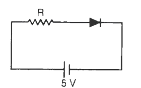
View SolutionThe diode used in figure requires minimum current of 1 mA to be above the knee voltage 0.7 of current versus voltage characteristics. The maximum value of R so that the voltage is above knee point is :
View SolutionA piece of copper and another of germanium are cooled from room temperature to 80 K. The resistance of
View SolutionAn intrinsic semiconductor has `10^8 m^-3` free electrons and is doped with pentavalent impurity atoms of density `10^24 m^-3`. The free electron density will increase by ........ orders of magnitude.
View SolutionIn a p-n junction diode, the increase in forward voltage of 0.19V increases the forward current by 37.6 mA, The dynamic resistance of the junction is
View SolutionGiven sets of elements are phosphorus , arsenic , indium and bismuth . The addition of which in pure semiconductor will result in p - type semiconductor :
View SolutionVan der Waal's crystal are :
View SolutionThe symbol represents :

View SolutionNAND and NOR gates are called universal gates because they
View SolutionThe forbidden energy gap in conductors , semiconductors and insulators are `EG_1 , EG_2 and EG_3` respectively . The relation among them is :
View SolutionThe current gain `alpha` of a transistor is 0.95 . The change in emitter current is 10 mA. The change is base current is :
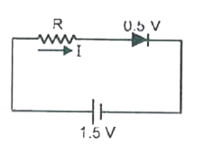
View SolutionThe diode used in the circuit shown in figure has a constant voltage drop at 0.5 V at all currents and a maximum power rating of 100 mW. What should be the value of the resistance R, connected in series with diode for obtaining maximum current ?
View SolutionVan der Waal's forces between atoms and between molecules arise from :
View SolutionThe coordination number for a simple cubic crystal is :
View SolutionIn molecular crystals , the force between molecules is
View SolutionAssuming that the silicon diode having resistance of `20Omega` , the current through the diode is (knee voltage 0.7 V) :
View SolutionIn a transistor `(beta = 45)`, the voltage across `5 kOmega` load resistance in collector circuit is 5 V. The base current is
View SolutionA `p` -type semiconductor has acceptor level 66 meV above the valence band. The maximum wavelength of light required to create a hole is very near to :
View SolutionIn which of the following cases the diode is forward biased ?
View Solution`n` type and `p` type semiconductors can be obtained by doping pure silicon respectively with
View SolutionThe number of terminals in a transistor is :
View SolutionTo produce N - type crystal Ge or Si may be doped with a substance that is :
View SolutionTransistor was invented by :
View SolutionThe forbidden energy gap in Ge in 0.72 eV Given, `hc=12400" eV"-Å` The maximum wavelength of radiation that will generate electron hole pair is
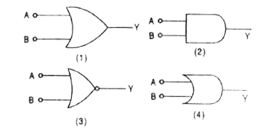
View SolutionGiven below are four logic gate symbols . Those for OR, NOR and NAND are respectively
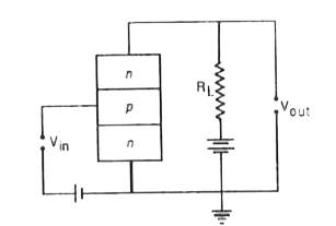
View SolutionAn n - p -n transistor circuit is arranged as shown in the figure , it is
View SolutionIf the current gain in CB configuration is 0.95. Then the current gain in CE configuration is
View SolutionWrite the expression for the frequency of an LC oscilator?
View SolutionIn the Binary number system the number 100 represents :
View SolutionOR gate operation means :
View SolutionUnder space charge limited conditions , the plate current in a diode is 10 mA at place potential of 100 V, If the plate potential is changed to 400 V, what is the plate current ?
View SolutionA triode valve has an amplification factor 20 and its plate potential is 300 V . What should be the grid potential to reduce the plate current zero ?
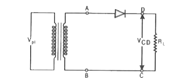
View SolutionIn the half - Wave rectifier circuit , which one of the following wave forms is true for `V_(CD)` , the output across C and D ?
View SolutionWhich of the following gates will have an output of 1 ?
View SolutionFor an electronic value the plate current `I_p` and the plate voltage `V_p` in the space charge limited region are related as :
View SolutionSrO (strontium oxide) is coated on tungsten for thermionic emission in values because :
View SolutionBy bringing the grid nearer to the plate in a triode value, the amplification factor :
View SolutionFor a CE transistor amplifier, the audio signal across the collector resistance of `2kOmega` is 2V. Suppose the current amplification factor of the transistor is 100, find the input signal voltage and base current, if the base resistance is 1 k`Omega`.
View SolutionTwo amplifiers are connected one after the other in series. The first amplifier has a voltage gain of 10 and the second has a voltage gain of 20. If the input signal is 0.01V. Calculate the output ac signal.
View SolutionA diode valve works in the region of space charge limited current . If the voltage is increased 4 times, how many times the space charge limited current will increase ?
View SolutionThe amplification factor of a triode is 20 . Its plate resistance is `10kOmega` . Its mutual conductance is :
View SolutionIn NOT operation of Y is output and A and B are inputs then truth table in
View SolutionIn a common - base circuit of transistor , current amplification factor is 0.95 Calculate the emitter current , if base current is 0.2 mA :
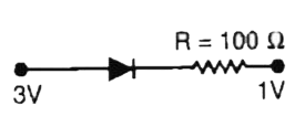
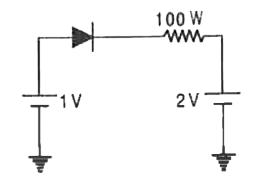
View SolutionAssuming that the junction diode is ideal , in the circuit shown here , the current through the diode is :
View SolutionIn the study of transistor as amplifier, if `alpha=I_C/I_E` and `beta=I_C/I_B`, where `I_C,I_B` and `I_E` are the collector, base and emitter currents, then
View SolutionThe forward biased diode is :
View SolutionThe number density of free electrons in the semiconductor is `10^(18) m^(-3)` . It is doped with a pentavalent impurity atoms of number density `10^(24) m^(-3)` . The number density of free electrons `m^(-3)` increases by a factor of
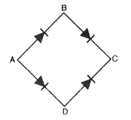
View SolutionTwo identical p - junctions may be connected in series with a battery in three ways as shown . The potential drops across the two p - n junctions are equal in :

View SolutionIn the Fig. the input is across A and C and output across B and D . The output is :
View SolutionIf the forward bias voltage a `p-n` junction diode is changed form 0.7 V to 2.2 V, the forward current changes by 1.5 mA, the forward resistance of diode is
View SolutionThe collector supply in a common emitter amplifier is 8V and the voltage drop across the load of `800 Omega` is 0.4 V. If the current gain for common base be `alpha = 0.96`, then the base current is
View SolutionWhen NPN transistor is used as an amplifier, then
View SolutionTo a germanium sample , pieces of gallium are added as an impurity . The resultant sample would behave like :
View SolutionA transistor has `alpha = 0.95` . The change in emitter current is 100 milliampere , then the change in the collector current is :
View SolutionThree amplifiers each with a voltage gain of 10 are connected in series. Then overall amplification is :
View SolutionFor common emitter circuit of a transistor , when the base current changes by `80 muA`, the collector current change by 4.8 mA. Then the current amplification factor will be :
View SolutionWhat is the voltage gain in a common emitter amplifier, where input resistance is `3 Omega` and load resistance `24 Omega, beta = 0.6` ?
View SolutionThe source voltage is 9 volt and source resistance is `1kOmega` The current through the silicon diode is (knee voltage of silicon is 0.7 volt):
View SolutionIf `l_1,l_2,l_3` are the lengths of the emitter, base and collector of a transistor, then
View SolutionIn an `n-p-n` transistor, the current gain for common emitter configuration is 80. If the emitter current be 8.1 mA, then base current is
View SolutionThe transfer ratio `beta` of a transistor is 50. The input resistance of the transistor when used in the common-emitter configuration is `1 kOmega`. The peak value of the collector ac current for an ac input voltage of 0.01 V peak is
View SolutionDecimal number 53 is equal to binary number
View SolutionThe energy gap is max in :
View SolutionFormation of covalent bonds in compounds exhibits :
View SolutionA transistor is connected in common emitter configuration . The collector emitter voltage is 8 V and a load resistance of `800 Omega` is connected in the collector circuit . The voltage drop across the load resistance is 0.5 V . If the current gain be 0.96 , the base current is :
View SolutionIn a common emitter amplifier output resistance is 5000 ohm and input resistance is 2000 ohm. If peak value of signal voltage is 10 mV and `beta = 50`, then the peak value of output voltage is :
View SolutionCopper and germanium are cooled to 70K from room temperature, then
View SolutionManifestation of band structure in solids is due to :
View SolutionThe current gain of a transistor is 100. If the base current changes by `200 muA`, what is the change in collected current ?
View SolutionWhat is the voltage gain of a transistor with load resistance `100 Omega` and internal resistance `200 Omega` ? Given that `beta = 90`.
View SolutionA solid which is not transparent to visible light and whose conductivity increases with temp is formed by
View SolutionIf the lattice constant of this semiconductor is decreased , then which of the following is correct ?
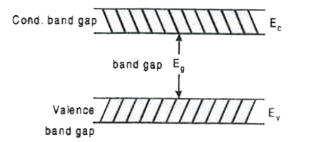
View SolutionWhich diode is reverse biased ?
View SolutionCarbon, silicon and germanium have four valence electrons each . At room temperature which one of the following statements is most appropriate ?
View SolutionIf in a p - n junction diode , a square input signal of 10 V is applied as shown :
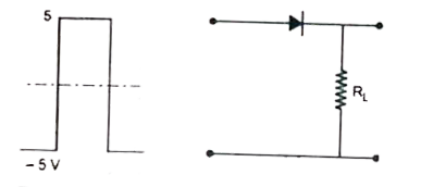
Then the output signal across `R_L` will be :
View SolutionA working transistor with its three legs marked , P Q and R is tested using a multimeter . No conduction is found between P and Q . By connecting the common (negative ) terminal of the multimeter to R and the other (positive) terminal to P or Q. some resistance is seen on the multimeter. Which of the following is true for the transistor ?
View SolutionIn the circuit below , A and B represent two inputs and C represents the output . The circuit represents
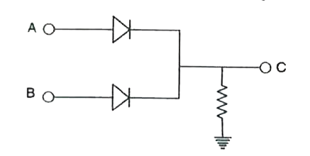
View Solution
Multiple Choice Questions - LEVEL -I questions and complete solutions for chapter SOLIDS & SEMICONDUCTOR DEVICES of MODERN PUBLICATION PHYSICS (KANNADA ENGLISH) of Class 12