Complete Solutions to Multiple Choice Questions - LEVEL -II of chapter SOLIDS & SEMICONDUCTOR DEVICES of Class 12 book with complete answers and questions
| Class 12 | PHYSICS |
| Chapter | SOLIDS & SEMICONDUCTOR DEVICES |
| MODERN PUBLICATION | Multiple Choice Questions - LEVEL -II |
| Number Of Questions | 58 |
| Academic Year | 2023-24 |
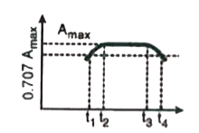
The frequency response curve of RC coupled amplifier is shown in figure . The band width of the amplifier will be :
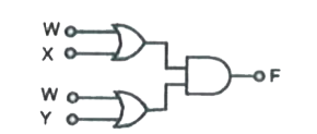
View SolutionThe diagram of a logic circuit is given below . The output F of the circuit is represented by :
View SolutionIf A is the atomic mass number of an element , N is the Avogardro number and a is the lattice parameter, then the density of the element , if it has crystal structure , is :
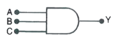
View SolutionThe output from a logic gate is 1 when inputs A, B and C are such that
View SolutionAn n - type semiconductor has resistivity `0.1Omegam` . The number of donor atoms which must be added to achieve this is ( `mu=0.05 m^2V^(-1)s^(-1)` ) :
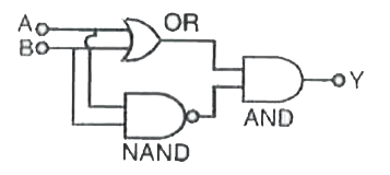
View SolutionThe following configuration of gate is equivalent to :
View SolutionThe binary number corresponding to the decimal number 49 is :
View SolutionIn AND operation if Y is output and A and B are inputs the truth table is :
View SolutionThe slope of `i_p-V_g` curve is 2 mA/V and slope of `i_p-V_p` curve is 0.25 mA/V . If anode resistance is `12KOmega` what amplification the triode value would produce across the load resistance ?
View SolutionWith 448 mW power used the number of electrons reaching the anode/sec is `1.4xx10^(16)` , then plate voltage is :
View SolutionTwo triodes A and B have plate amplifications factor of 40 . The plate resistance are `4kOmega and 8 kOmega` respectively. If an amplifier circuit is made using any one of them with a load with a load resistance of `8kOmega` , the ratio of voltage gain obtained from them will be :
View SolutionKeeping the grid voltage constant a change in the plate potential of 50 V, changes the plate current by 10 mA. And keeping the plate potential constant a change in the grid potential of 2V changes the plate current by 10 ma again , the amplification factor of the triode will be :
View SolutionFor a transistor the current amplification factor is 0.8 . If the transistor is now in common emitter configuration , the change in collector current when the base current changes by 6 mA is :
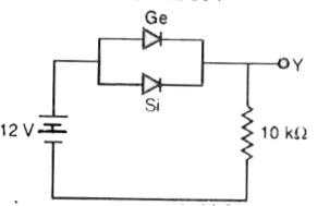
View SolutionTwo junction diodes one of germanium (Ge) and other of silicon (Si) are connected as shown in fig to a battery of e.m.f. 12 V and a load resistance `10kOmega` The germanium diode conducts at 0.3V and silicon diode at 0.7 V When a current flows in the circuit , the potential of terminal Y will be :
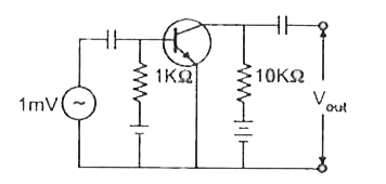
View SolutionIn the following common emitter configuration an NPN transistor with current gain `beta = 100` is used . The output voltage of the amplifier will be
View SolutionA Ge specimen is doped with Al. The concentration of acceptor atoms is `~10^(21)` atoms/ `m^3` . Given that the intrinsic concentration of electron hole Paris is `~10^(19)//m^3` , the concentration of electrons in the specimen is :
View SolutionThe diode used in the circuit shown in figure has a constant voltage drop at 0.5 V at all currents and a maximum power rating of 100 mW. What should be the value of the resistance R, connected in series with diode for obtaining maximum current ?
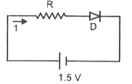
View SolutionIn an n-p-n transistor circuit, the collector current is 10mA. If 90% of the electrons emitted reach the collector, the emitter current `(I_(E ))` and base current `(I_(B))` are given by
View SolutionA transistor with `alpha = 0.98 ` is operated in common emitter circuit with a load resistance of `5kOmega` . If the dynamic resistance of the base emitter junction is `7Omega` , the voltage gain and power gain will be :
View SolutionIn a common emitter amplifier output resistance is 2000 ohm and input resistance is 5000 ohm. The input signal is of 10 mV and `beta=50`,
Then output voltage is
View SolutionIn a common emitter amplifier output resistance is 2000 ohm and input resistance is 5000 ohm. The input signal is of 10 mV and `beta=50`,
Then power gain is
View SolutionA n-p-n transistor is connected in C - E configuration Collector supply is 8 V . The voltage drop across the load resistor of `800Omega` , connected to collector circuit is 0.8 volt . If `alpha = 25/26`
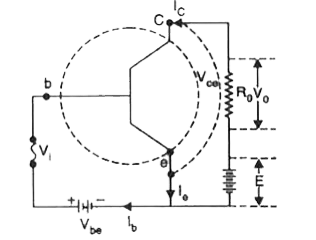
Then collector emitter voltage `(V_("ce"))` is
View SolutionA n-p-n transistor is connected in C - E configuration Collector supply is 8 V . The voltage drop across the load resistor of `800Omega` , connected to collector circuit is 0.8 volt . If `alpha = 25/26`
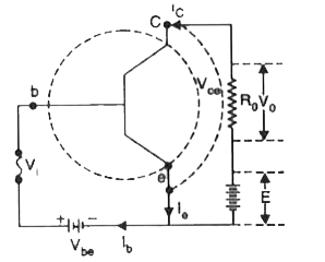
If input resistance of transistor is `200Omega` , then power gain is
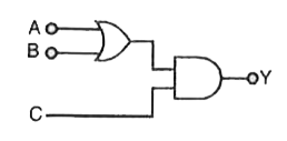
View SolutionTo get an output Y = 1 from circuit of figure, the inputs must be :
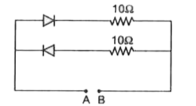
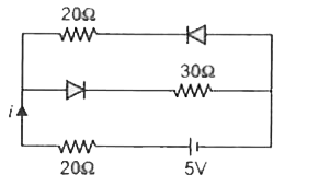
View SolutionA 2V battery is connected across the points A and B as shown in the figure given below . Assuming that the resistance of each diode is zero in forward bias and infinity in reverse bias , the current supplied by the battery when its positive terminal is connected to A is
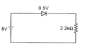
View SolutionIn the circuit , if the forward voltage drop for the diode is 0.5 V , the current will be
View SolutionA P - type semiconductor has acceptor level 57 meV above the valence band. The maximum wavelength of light required to create a hole is (Planck's constant `h=6.6 xx10^(-34) J-s`)
View SolutionCurrent in the circuit will be :
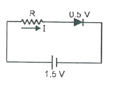
View SolutionThe diode used in the circuit shown in figure has a constant voltage drop at 0.5 V at all currents and a maximum power rating of 100 mW. What should be the value of the resistance R, connected in series with diode for obtaining maximum current ?
View SolutionIn the following common emitter configuration an NPN transistor with current gain `beta = 100` is used . The output voltage of the amplifier will be

View SolutionA sinusoidal voltage of Peak value 200 volt is connected to a diode and resistor R in the circuit shown so that half wave rectification occurs . If the forward resistance of the diode is negligible compared to R the rms (in volt) across R is approximately

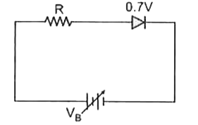
View SolutionThe junction diode in the following circuit requires a minimum current of 1 mA to be above the knee point (0.7V) of its 1-V characteristic curve . The voltage across the diode is independent of current above the knee point . If `V_B = 5V` , then the maximum value of R so that the voltage is above the knee point will be
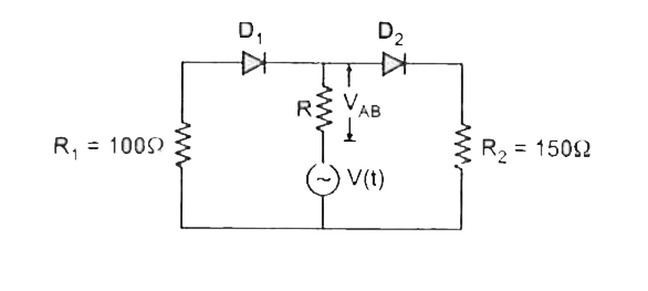
View SolutionIn the circuit given below , V(t) is the sinusoidal voltage source , voltage drop `V_(AB)(t)` across the resistance R is
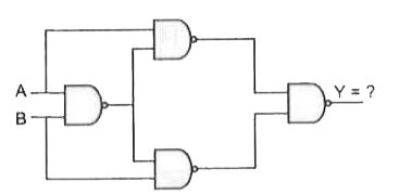
View SolutionSelect outputs Y of the combination of gates shown below for inputs A = 1 , B = 0 , A = 1 , B = 1 and A = 0 , B = 0 respectively.
View SolutionIn the following circuits PN - junction diodes `D_1,D_2 and D_3` are ideal for the following potentials of A and B. The correct increasing order of resistance between A and B will be
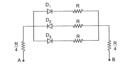
(i) `-10V, -5V`
(ii) `-5 V,-10V`
(iii) `-4V,-12V`
View SolutionFind `V_(AB)`

View SolutionA diode is connected to 200 V (rms) ac in series with a capacitor as shown in figure. The voltage across the capacitor is

View SolutionA potential difference of 2V is applied between the opposite faces of a Ge crystal of area ` 1 cm^2` and thickness 0.5 mm . If the concentration of electrons in Ge is `2xx10^(19)//m^3` and mobilities of electrons and holes are `0.36(m^2)/("volt"-s) and 0.14(m^2)/("volt"-s)` respectively , then the current flowing through the plate will be
View SolutionThe contribution in the total current flowing through a semiconductor due to electrons and holes are `3/4 and 1/4` respectively . If the drift velocity of electrons is `5/2` times that of holes at this temperature, then the ratio of concentration of electrons and holes is
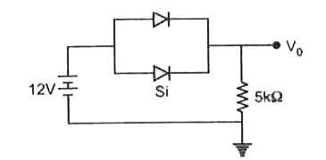
View SolutionGe and Si diode conduct at 0.3 V and 0.7respectively . In the following figure if Ge diode connection is reversed, the value of `V_0` changes by
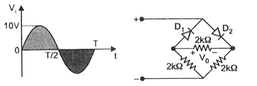
View SolutionIn the circuit shown in figure the maximum output voltage
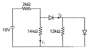
View SolutionIn the following circuit find `I_1 and I_2`
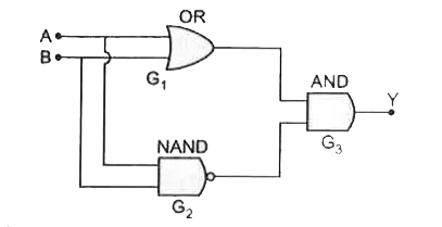
View SolutionThe following configuration of gate is equivalent to :
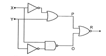
View SolutionFigure gives a system of logic gates . From the study of truth table it can be found that to produce a high output (1) at R , we must have
View SolutionThe combination of gates shown below produces
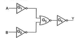
View SolutionThe figure shows NAND gates followed by a NOR gate . The system is equivalent to the following logic gate .
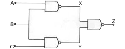
View SolutionThe diagram of a logic circuit is given below . The output F of the circuit is represented by :

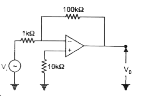
View SolutionThe voltage gain of the following amplifier is
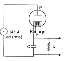
View SolutionAn alternating voltage of 141.4 V (rms) is applied to a vacuum diode as shown in the figure. The maximum potential difference across the condenser will be
View SolutionThe plate current in a triode is given be `I_p=0.004 (V_p+10V_g)^(3//2)mA`
where `I_p,V_p and V_g` are the values of plate current , plate voltage and grid voltage , respectively. What are the triode parameters `mu,r_p and g_m` for the operating point at `V_p = 120 ` volt and `V_g =-2` volt
View SolutionFor an amplifier in C.E. configuration for load `1kOmega (h_(fe)=50) and (h_("cc")=25xx10^(-6))` , the current gain is :
View SolutionIn a full wave rectifier with input frequency 50 Hz the ripple in the output is mainly of the frequency (in Hz)
View SolutionThe electrical conductivity of a semiconductor increases when electromagnetic radiation of wavelength shorter than 2480 nm is incident on it. The band gap (in eV) for semi-conductor is
View SolutionIf ratio of concentration of electrons to that of holes in a semiconductor is 7/5 and the ratio of currents is 7/4 , what is the ratio of their drift velocities ?
View SolutionIn a common base mode of a transistor, the collector current is 5.488 mA for an emitter current of 5.60 mA. The values of the base - current amplification factor `(beta)` will be :
View SolutionA p - n junction (D) shown in the figure can act as a rectifier . An alternating current source (V) is connected in the circuit.
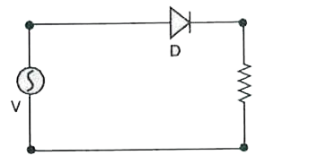
The current (I) in the resistor (R) can be shown by :
View SolutionThe logic circuit shown below has the input waveform 'A' and 'B' as shown . Pick out the correct output waveform .
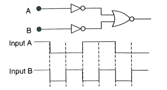
output is :
View SolutionThe combination of gates shown below yields :
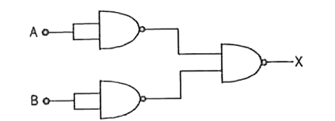
View Solution
Multiple Choice Questions - LEVEL -II questions and complete solutions for chapter SOLIDS & SEMICONDUCTOR DEVICES of MODERN PUBLICATION PHYSICS (KANNADA ENGLISH) of Class 12