Complete Solutions to Nuclei of chapter NUCLEI of Class 12 book with complete answers and questions
| Class 12 | PHYSICS |
| Chapter | NUCLEI |
| NCERT EXEMPLAR | Nuclei |
| Number Of Questions | 40 |
| Academic Year | 2023-24 |
Suppose we consider a large number of continers each containing initially `10000` atoms of a radioactive material with a half life of `1` year. After `1` year.
04:59View SolutionThe gravitational force between a H-atom and another particle of mass m will be given by Newton's law: `F=G (M.m)/(r^(2)`, where r is in km and
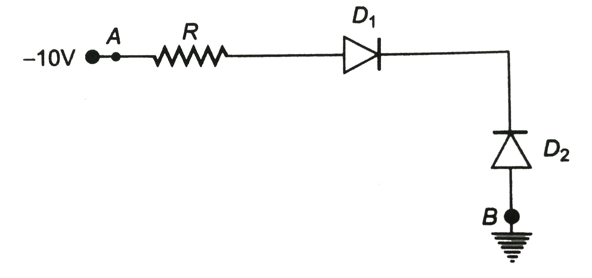
01:41View SolutionIn figure , assuming the diodes to be ideal ,
 02:08View Solution
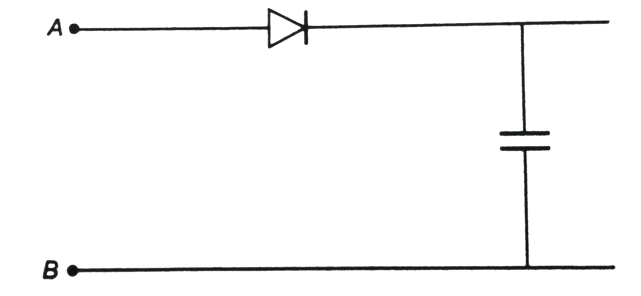
A 220 V AC supply is connected between points A and B . What will be the potential difference V across the capacitor ?
 01:35View Solution
Hole is
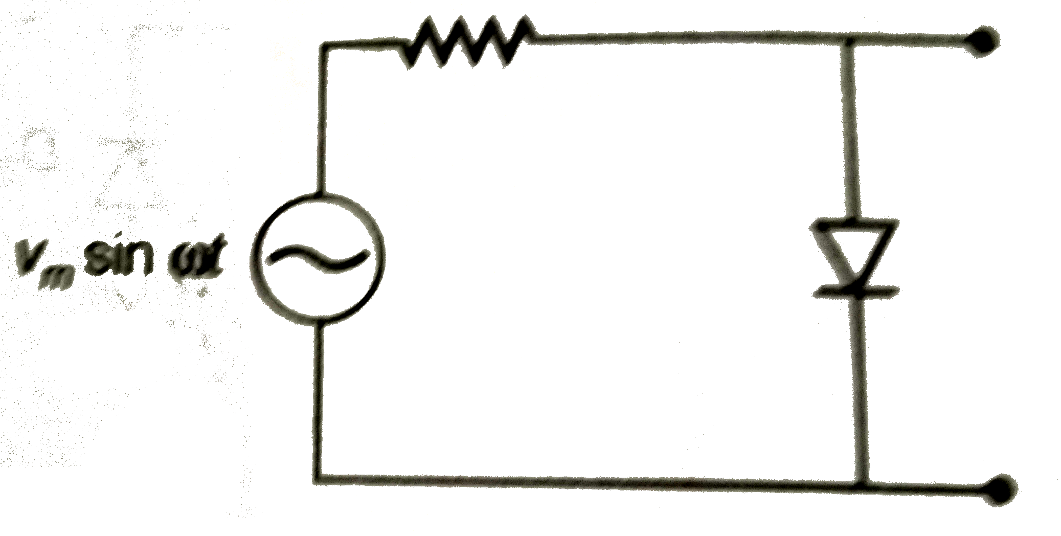
02:12View SolutionThe output of the given circuit in figure given below,
 04:28View Solution
In the circuit shown in figure, if the diode forward voltage drop is 0.3 V, then the voltage difference between A to B is,
 00:59View Solution
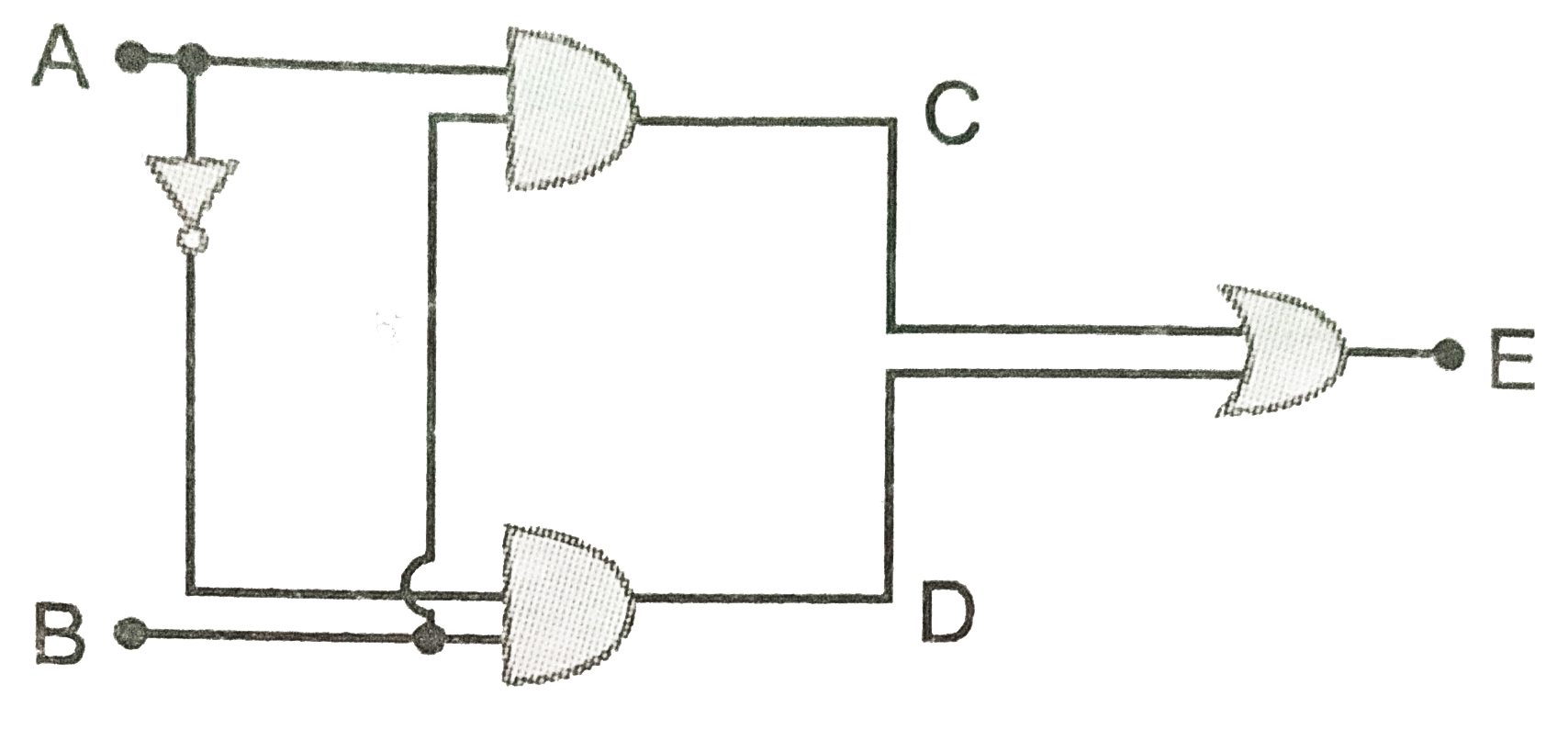
Truth table for the given circuit (Fig.)is
 03:02View Solution
When an electric field is applied across a semiconductor,
03:45View SolutionConsider an n-p-n transistor with its base - emitter junction forward biased and collector base junction reverse biased . Which of the following statements are true?
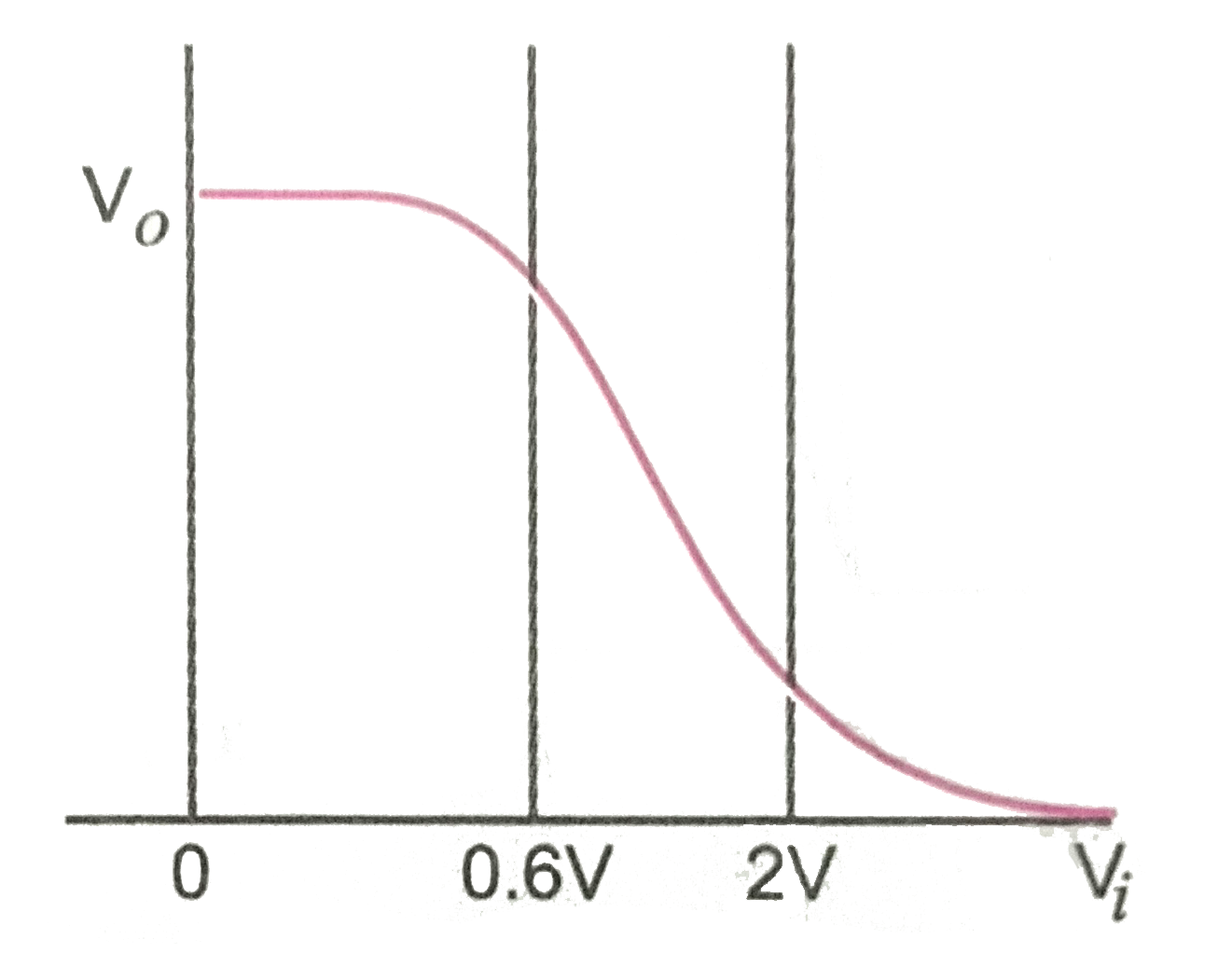
05:07View SolutionFig.shows that transfer characteristics of a base biased CE transistor. Which of the following statements are true?
 06:19View Solution
In a `n - p - n` transistor circuit, the collector current is `10 mA`. If 95 per cent of the electrons emitted reach the collector, which of the following statements are true ?
01:05View SolutionIn the depletion region of a diode.
05:32View SolutionWhat happens during regualtion action of a Zener diode?
02:51View SolutionTo reduce the ripples in rectifier circuit with capacitor filter
04:03View SolutionThe breakdown in a reverse biased p-n junction diode is more likely to occur due to
05:50View SolutionWhy are elemental dopants for Silicon or Germanium usually chosen from group XIII or group XV?
01:53View SolutionSn, C, Si and Ge are all group XIV elements . Yet , Sn is a conductor , C is an insulator while Si and Ge are semiconductors . Why?
03:36View SolutionCan the potential barrier across a `p - n` junction be measured by simply connecting a voltmeter across the junction ?
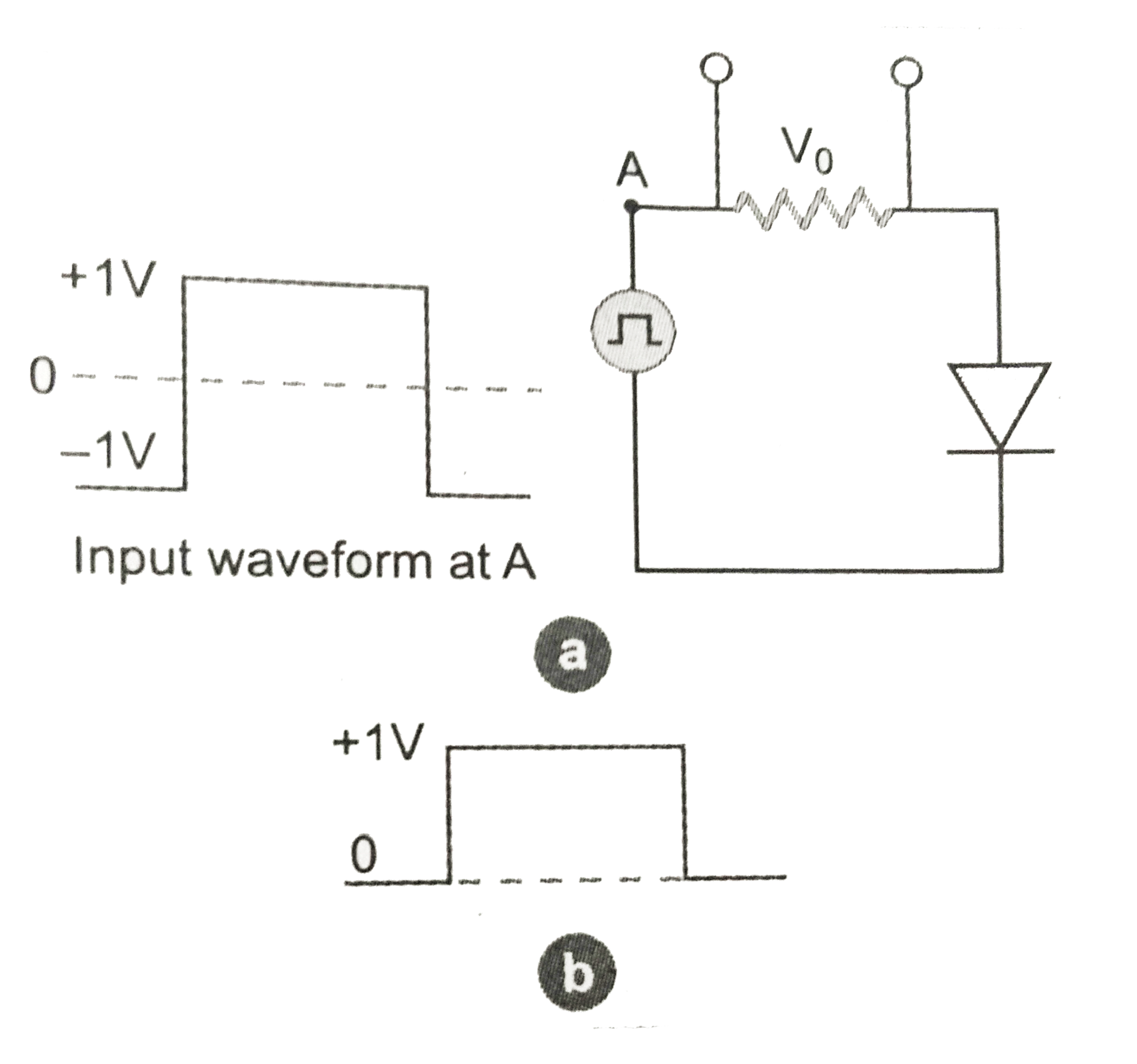
00:58View SolutionDraw the output waveform across the resistor (Fig.)
 01:31View Solution
The amplifiers `X, Y` and `Z` are connected in series. If the voltage gains of `X, Y` and `Z` are `10, 20` and `30`, respectively and the input signal is `1mV` peak value, then what is the output signal voltage (peak value)
(i) if dc supply voltage is 10V ?
(ii) if dc supply voltage is 5V?03:48View SolutionIn a CE transistor amplifier, there is a current and voltage gain associated with the circuit. In other words there is a power gain. Considering power a measure of energy, does the circuit violate conservation of energy ?
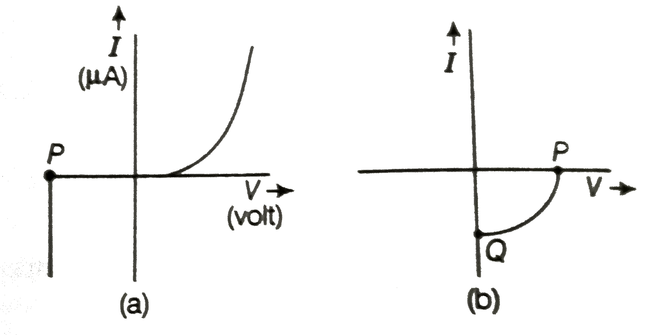
01:13View Solution(i) Name the type of a diode whose characteristics are shown in figure (a) and (b)
(ii) What does the point P in fig. (a) represent ?
(iii) What does the point P and Q in fig. (b) represent ?
 06:31View Solution
Three photodiodes `D_1 , D_2 ` and `D_3` are made of semiconductors having
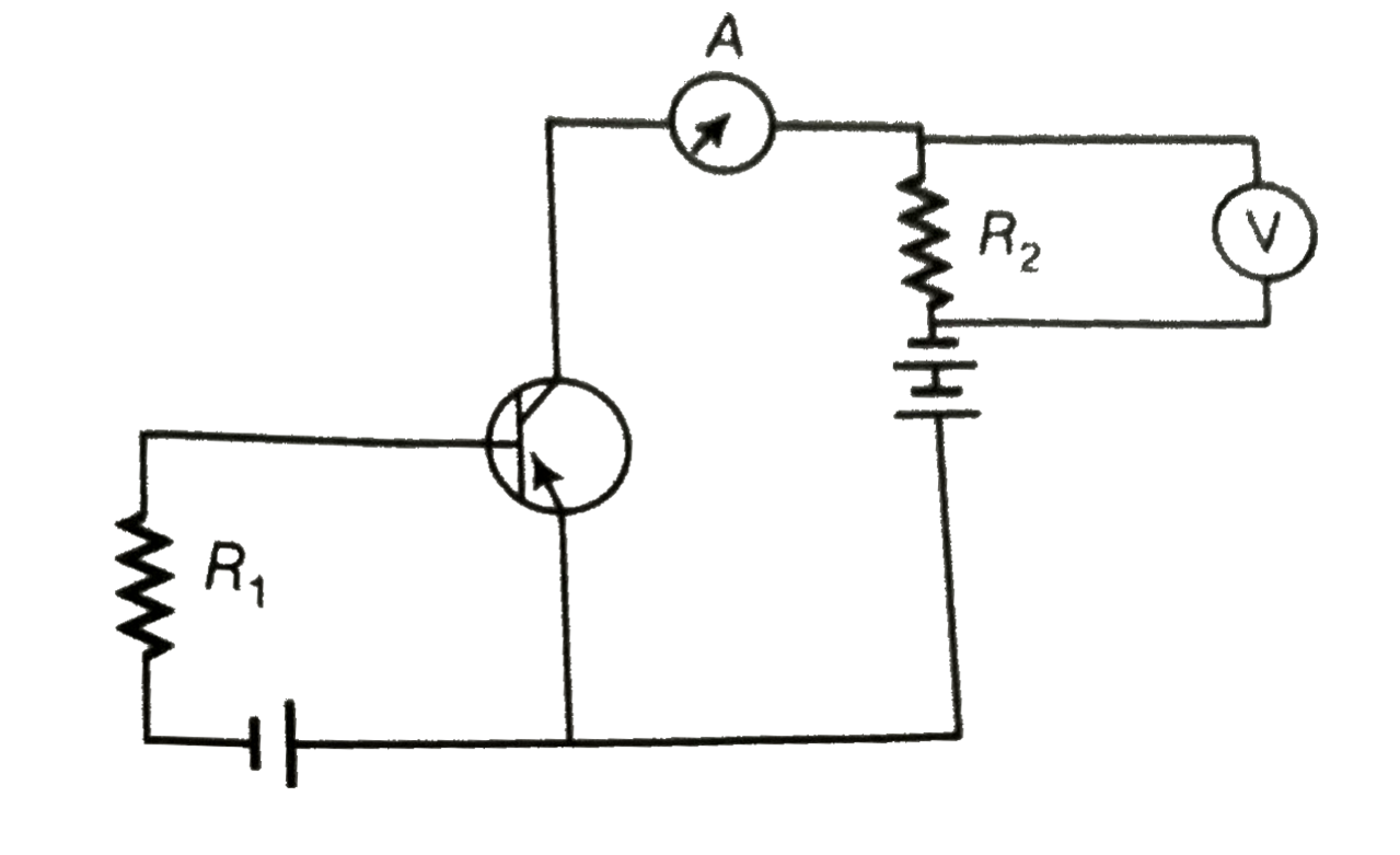
band gaps of ` 2.5 eV , 2 eV` and 3 eV , respectively . Which one will be able to detect light of wavelength ` 6000 Å ` ?02:25View SolutionIf the resistance `R_(1)` is increased (see figure), how will the reading of the ammeter and voltmeter change ?
 02:31View Solution
Two car garages have a common gate which needs to open automatically when a car enters either of the garages or cars enter both. Devise a circuit that resembles this situation using diodes for the situation .
04:25View SolutionHow would you set up a circuit to obtain NOT gate using a transistor?
01:54View SolutionExplain why elemental semiconductor cannot be used to make visible LEDs.
01:40View SolutionWrite the truth table for the circuit shown in figure given below. Name the gate that the circuit resembles.
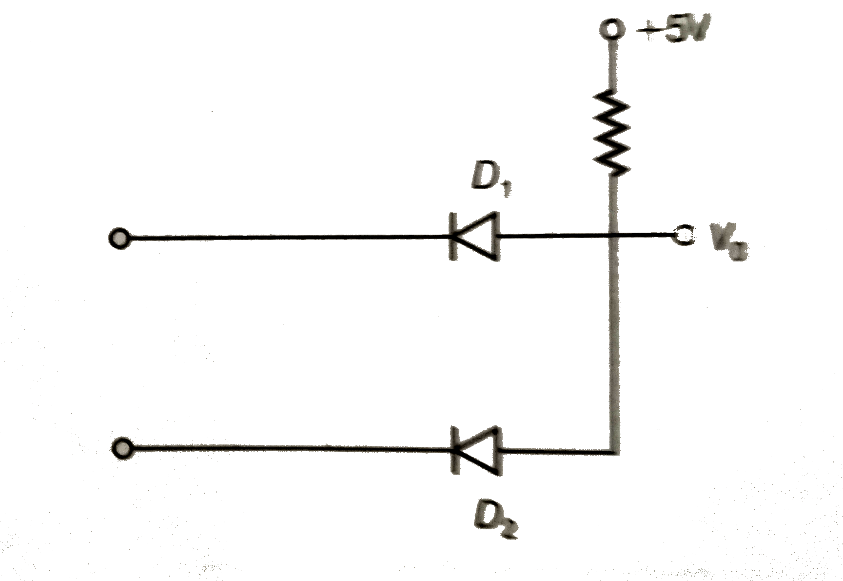 04:05View Solution
A Zener of power rating 1 W is to be used as a voltage regulator. If Zener has a breakdown of 5V and it has to regulate voltage which fluctuated between 3 V and 7 V, what should be the value of `R_(s)` for safe operation (see figure) ?
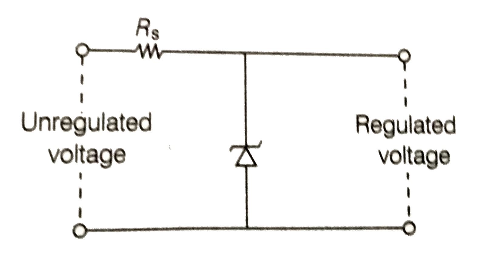 01:25View Solution
If each diode in figure has a forward has a forward bias resistance of 25 Omega and infinite resistance in reverse bias, what will be the values of the current ` I_1 , I_2 , I_3 and I_4? `
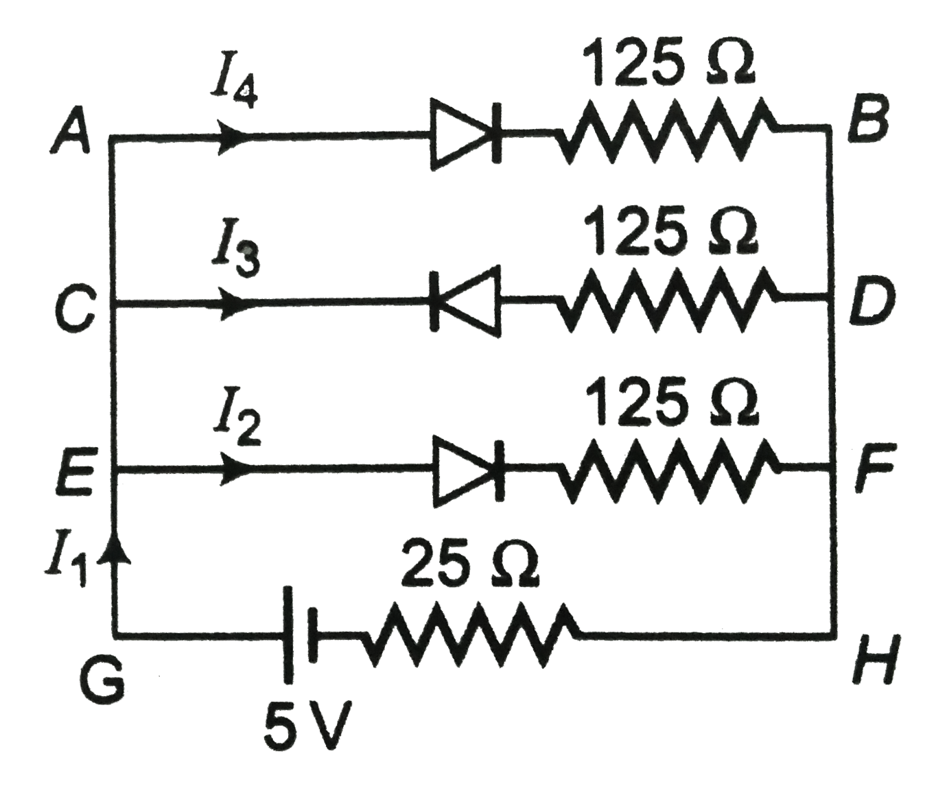 08:43View Solution
In the circuit shown in Fig. when the input voltage of the base resistance is `10V, V_(be)` is zero and `V_(ce)` is also zero. Find the values of `I_, I_` and `beta`.
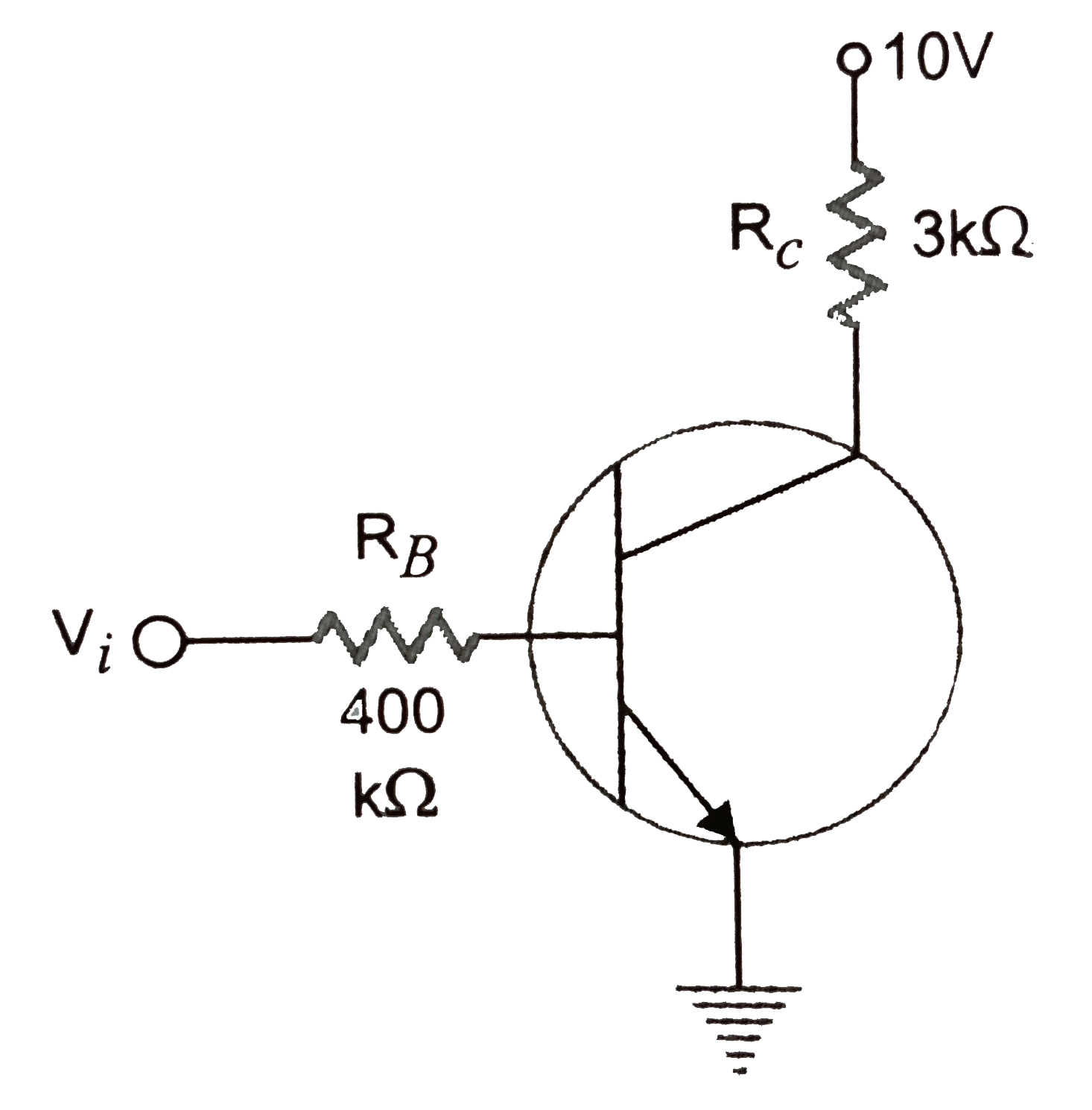 03:26View Solution
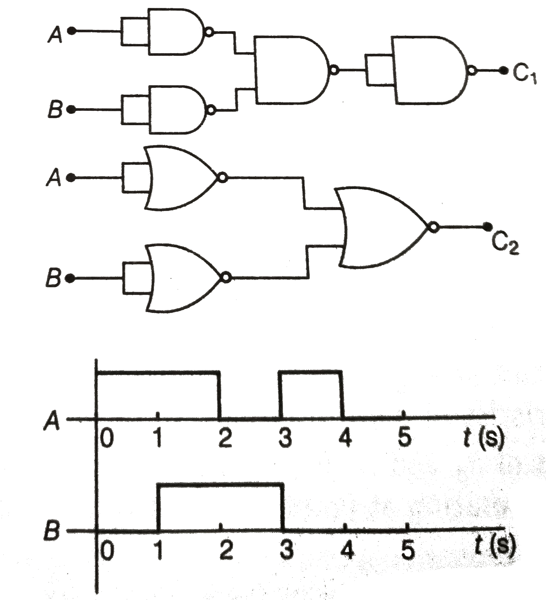
Draw the output signals `C_(1) " and " C_(2)` in the given combination of gates.
 05:33View Solution
Consider the circuit arrangnent shown in Fig. for studying input and output characteristics of npn transistor in CE configuration.
Select the values of `R_` and `R_` for a transistor whose `V_(BE)=0.7V`, so that the transistor is operating at point Q as shown in the characteristics shown in Fig.
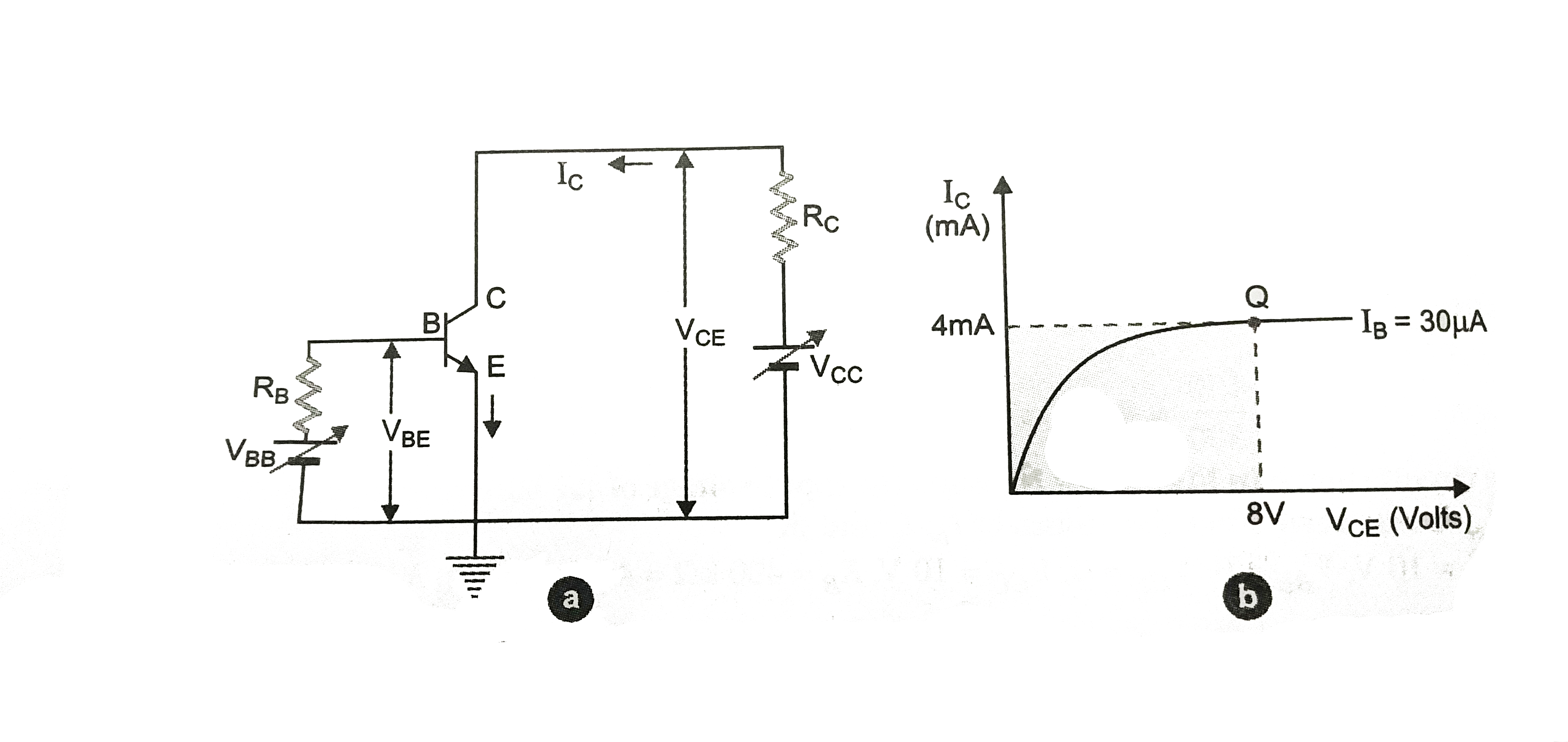 Given that the input impedance of the transistor is very small and `V_(C C)=V_(BB)=16V`, also find the voltage gain and power gain of circuit making appropriate assumptions.05:56View Solution
Assuming the ideal diode, draw the output waveform for the circuit given in fig. (a), explain the waveform
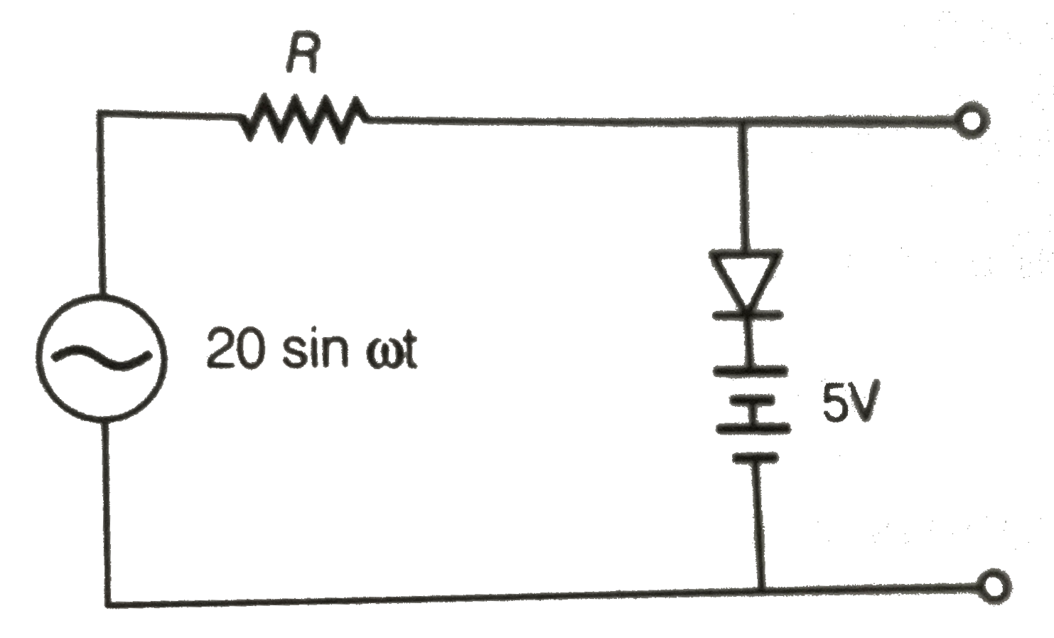 05:29View Solution
Suppose a 'n'- type wafer is created by doping Si crystal having `5xx10^(28) "atoms"//m^(3)` with 1 ppm concentration of As. On the surface 200 ppm Boron is added to create 'p' region in this wafer. Considering `n_(i)=1.5xx10^(16)m^(-3)`, (i) Calculate the densities of the charge carriers in the n & p regions. (ii) Comment which charge carriers would contribute largely for the reverse saturation current when diode is reverse biased.
06:00View SolutionAn X-OR gate has following truth table:
It is represented by following logic relation
`y=barA.B+A.barB`
Build this gate using AND, OR and NOT gates.
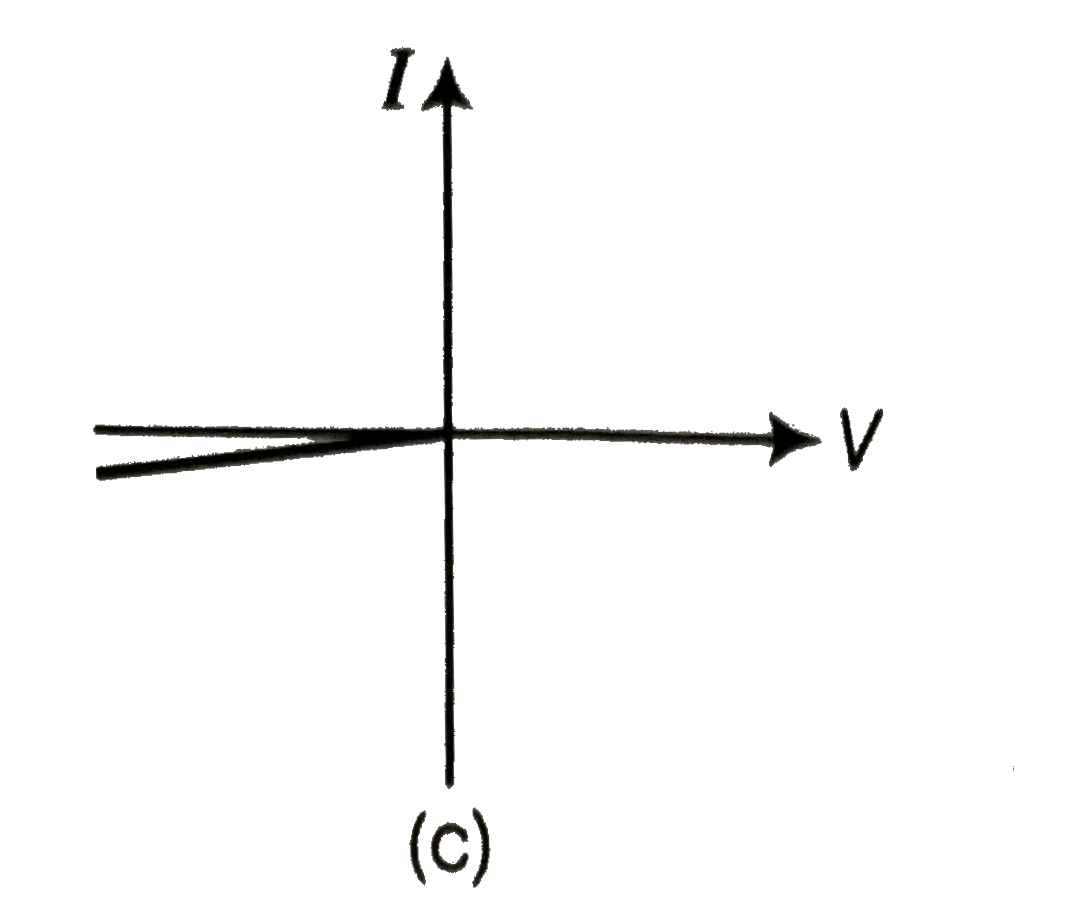
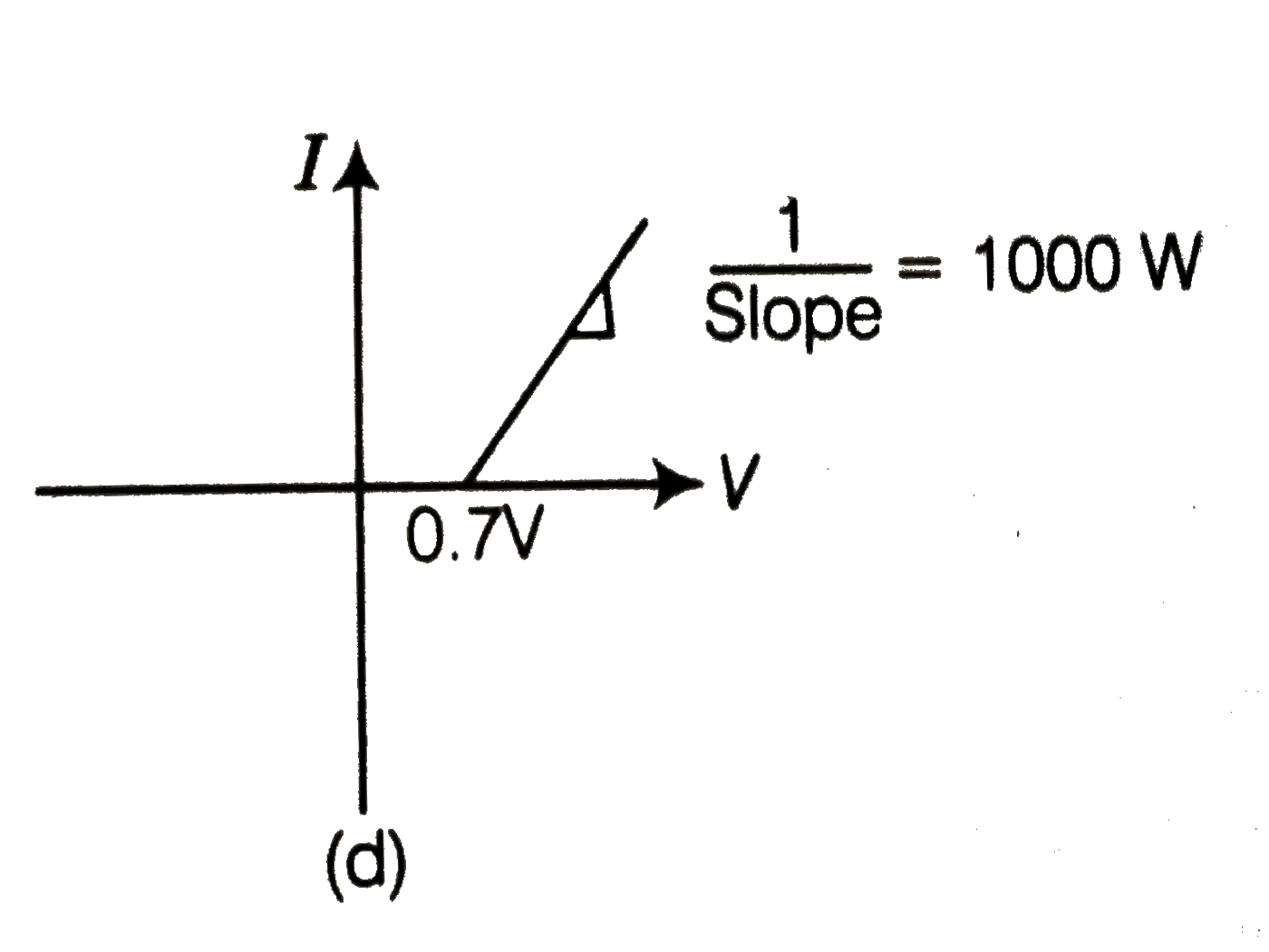
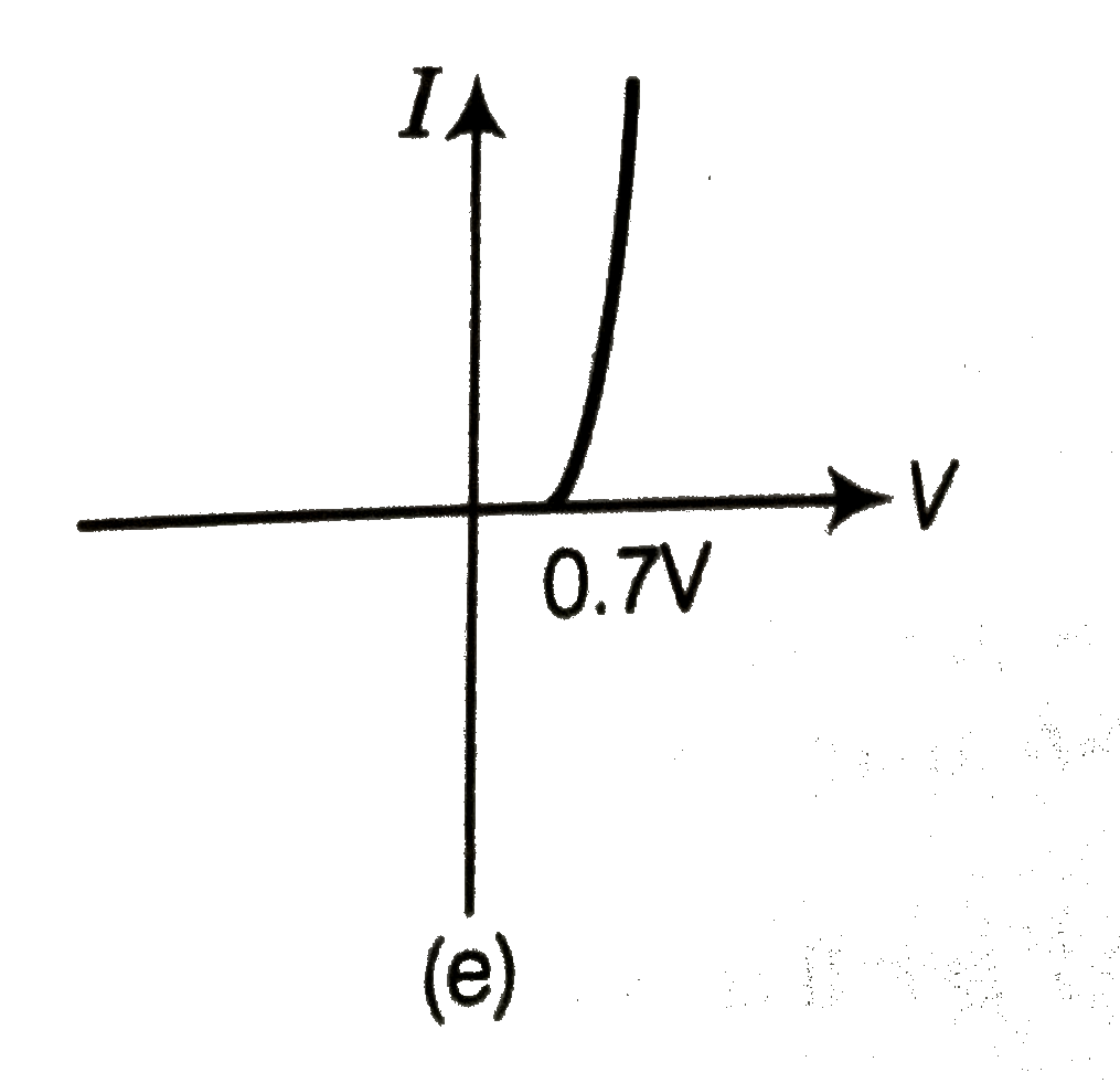
`|{:(A,B,Y),(0,0,0),(0,1,1),(1,0,1),(1,1,0):}:|`03:21View SolutionConsider a box with three terminals on top of it as shown in figure.
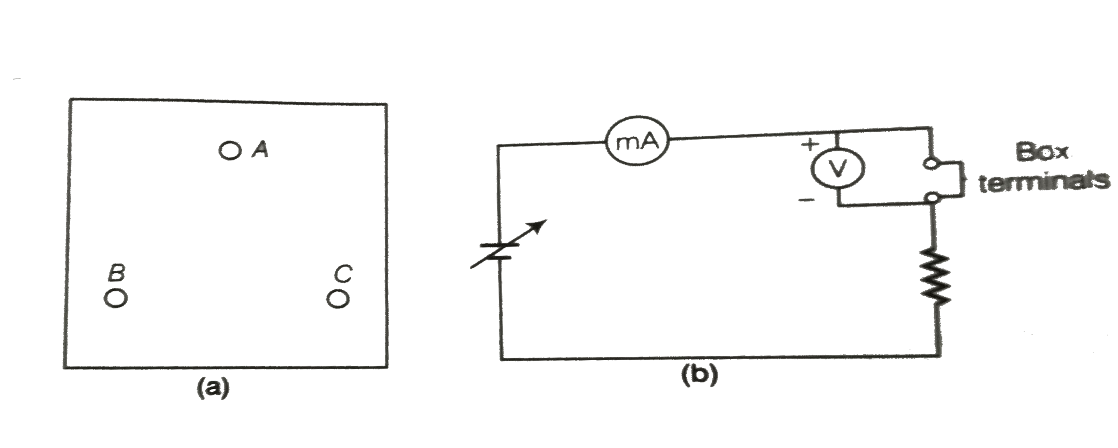
Three components namely, two germanium diodes and one resistor are connected across these three terminals in some arrangement
A student performs an experiment in which any two of these three terminals are connected in the circuit shown in figure.
The student obtains graphs of current-voltage characteristics for unknown combination of components between the two terminals connected in the circuit. The graphs are
(i) When A is positive and B is negative
(ii) When A is negative and B is positive
(iii) When B is negative and C is positve
(iv) When B is positive and C is neagtive
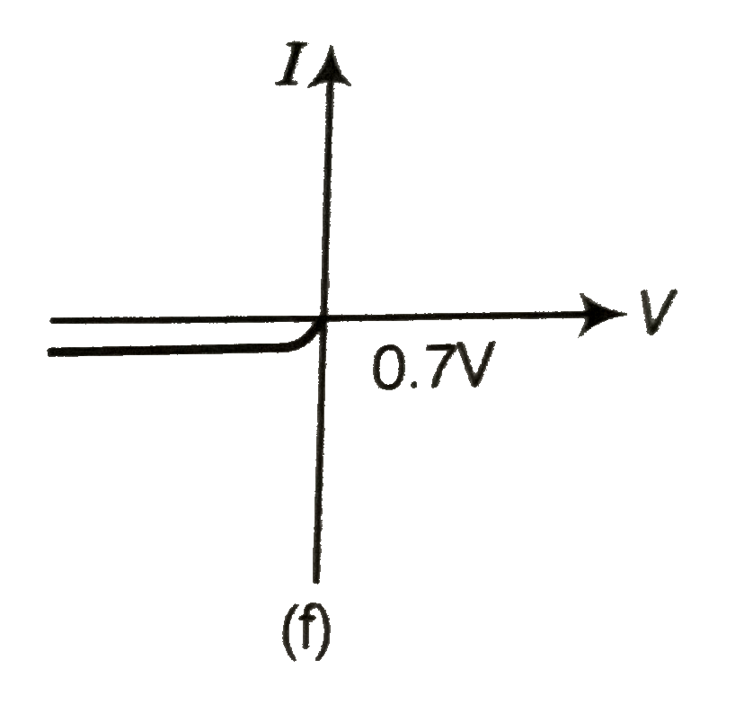
(v) When A is positive and C is negative
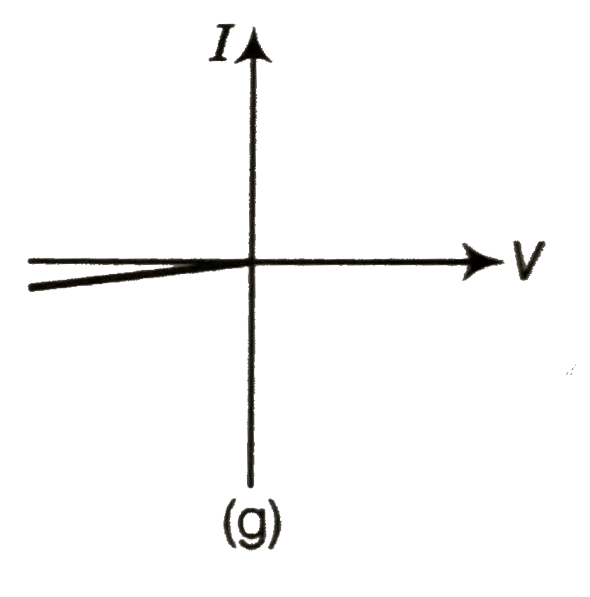
(vi) When A is negative and C is positive
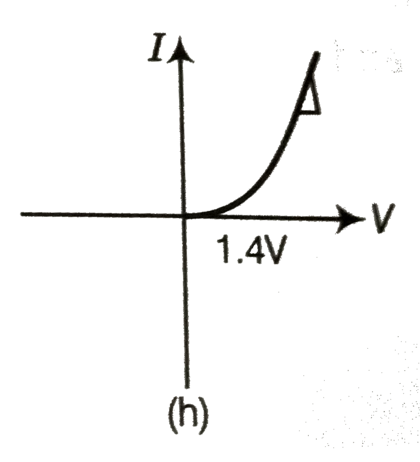
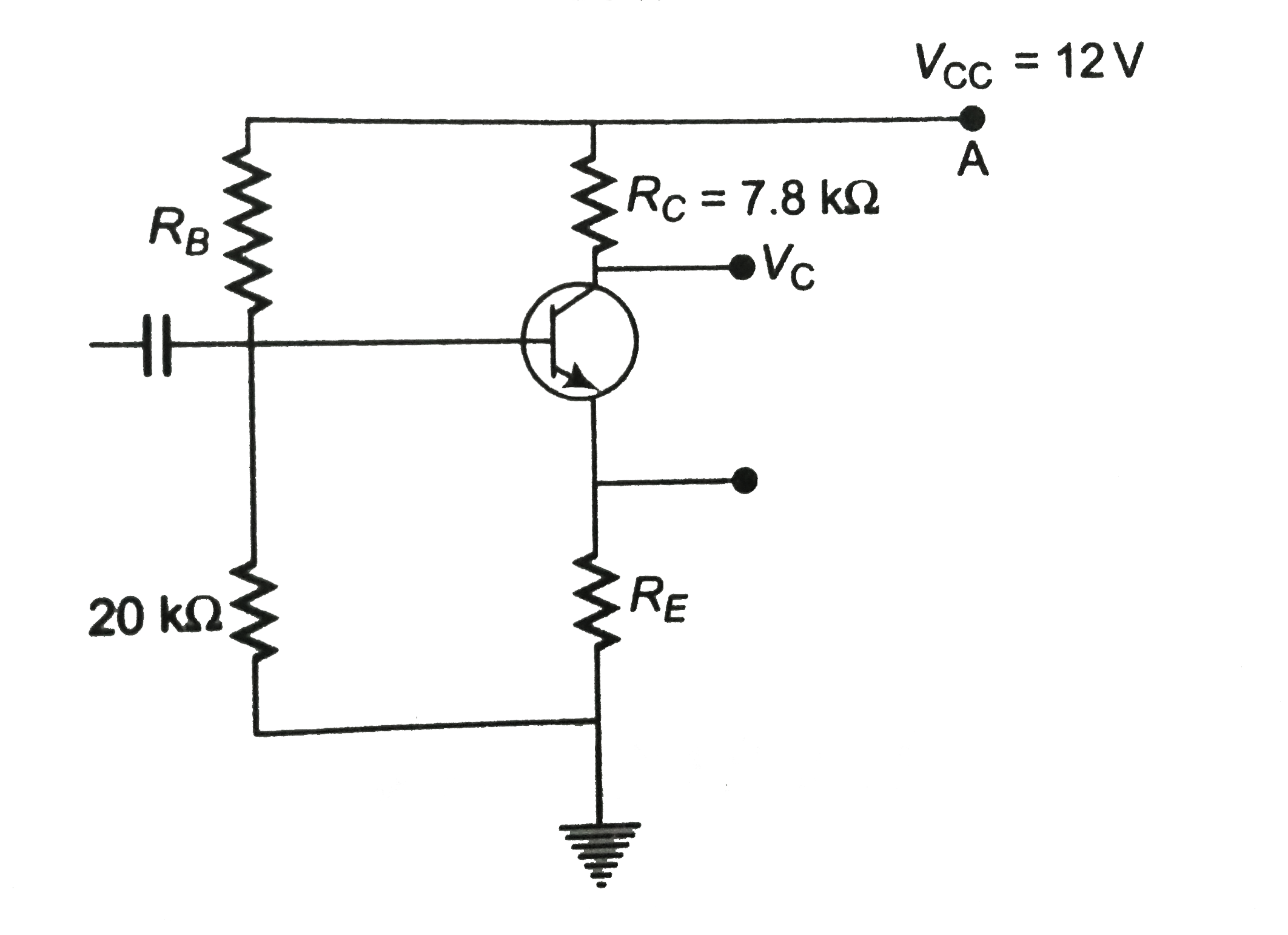
From these graphs of current `-` voltage characteristic shown in fig. (c) to (h) determine the arrangement of components between A, B and C.05:00View SolutionFor the transistor circuit shown in figure , evaluate `V_E , R_B and R_E`. Given `I_C = 1 mA`,
` V_(CE) = 3V , V_(BE) = 0.5 V , V_(CC )= 12 V and beta = 1000`
 07:10View Solution
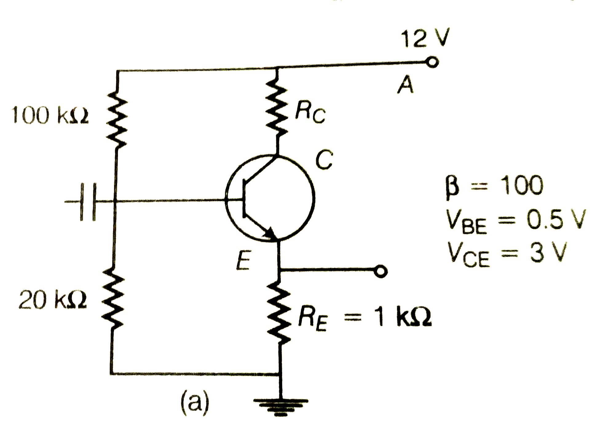
In the circuit shown in fig. (a), final the value of `R_(C)`.
 View Solution
Nuclei questions and complete solutions for chapter NUCLEI of NCERT PHYSICS (HINGLISH) of Class 12
