(a) Draw the circuit diagram of a full wave rectifier using p-n junction diole. Explain its working and show the output, input waveforms.
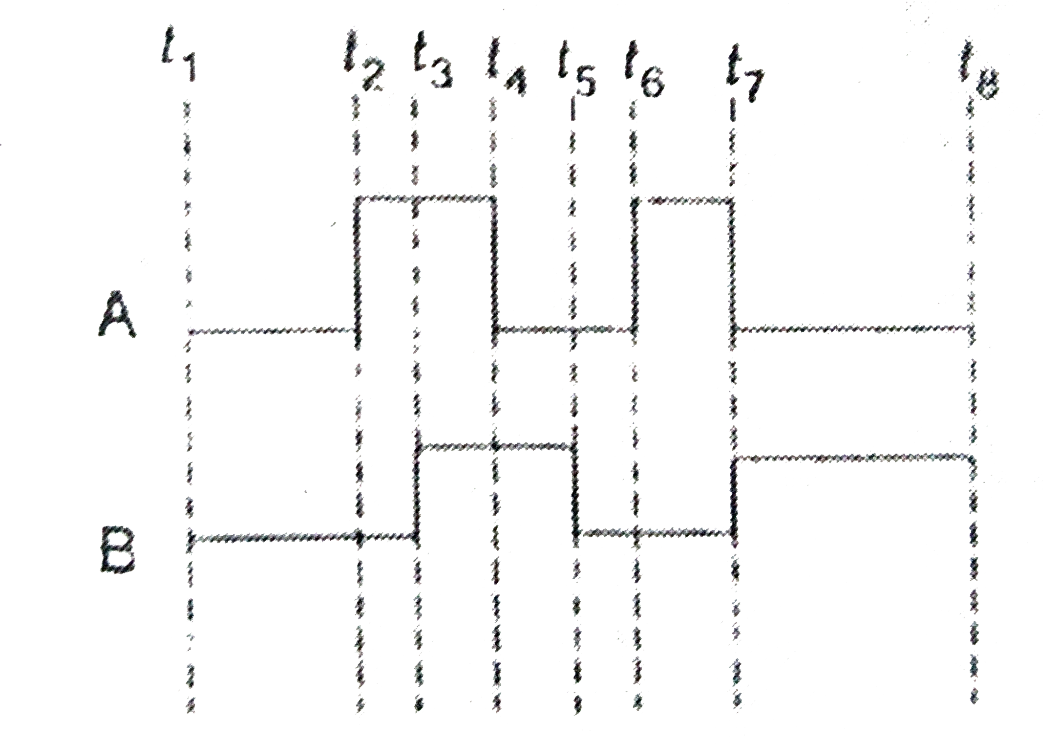
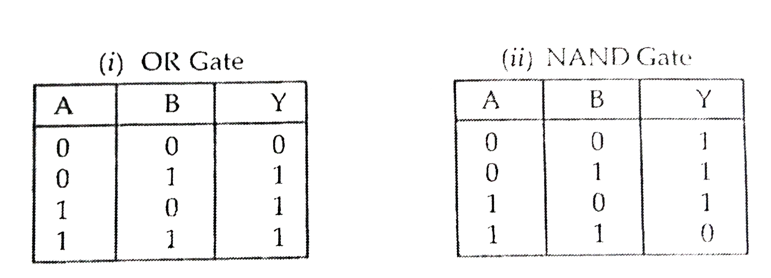
(b) Show the output waveforms (Y) for the following inputs A and B of (i) OR gate (ii) NAND gate :
(a) Full wave rectification : The circuit uses two diodes connected to the ends of a centre tapped transformer. The voltage rectified by the two diodes is half of the secondary voltage i.e., each diode conducts for half cycle of input but alternately so that output across load comes as half sinusoids with positive values only. For positive cycle diode Dt conducts (FB) but D2 is being out of phase is reverse biased and does not conduct. Thus, output across RL is due to D1 only. In negative cycle of input D1 is R.B. But D2 is F.B. and conducts as with respect to centre tap point A is negative but B is positive.
Hence, output across RL is due to D2.

Similar Questions
Draw circuit diagram for a full wave rectifier and show input output voltages.
View SolutionDraw the circuit diagram of half wave rectifier, showing input and output voltages.
View SolutionDraw the circuit diagram of a full wave rectifier. Explain its working showing its input and output waveforms.
View SolutionShow the output waveform of OR gate for the following input waveforms of A and B

View SolutionShow the output waveform of OR gate for the following input waveforms of A and B

View SolutionShow the output waveform of OR gate for the following input waveforms of A and B
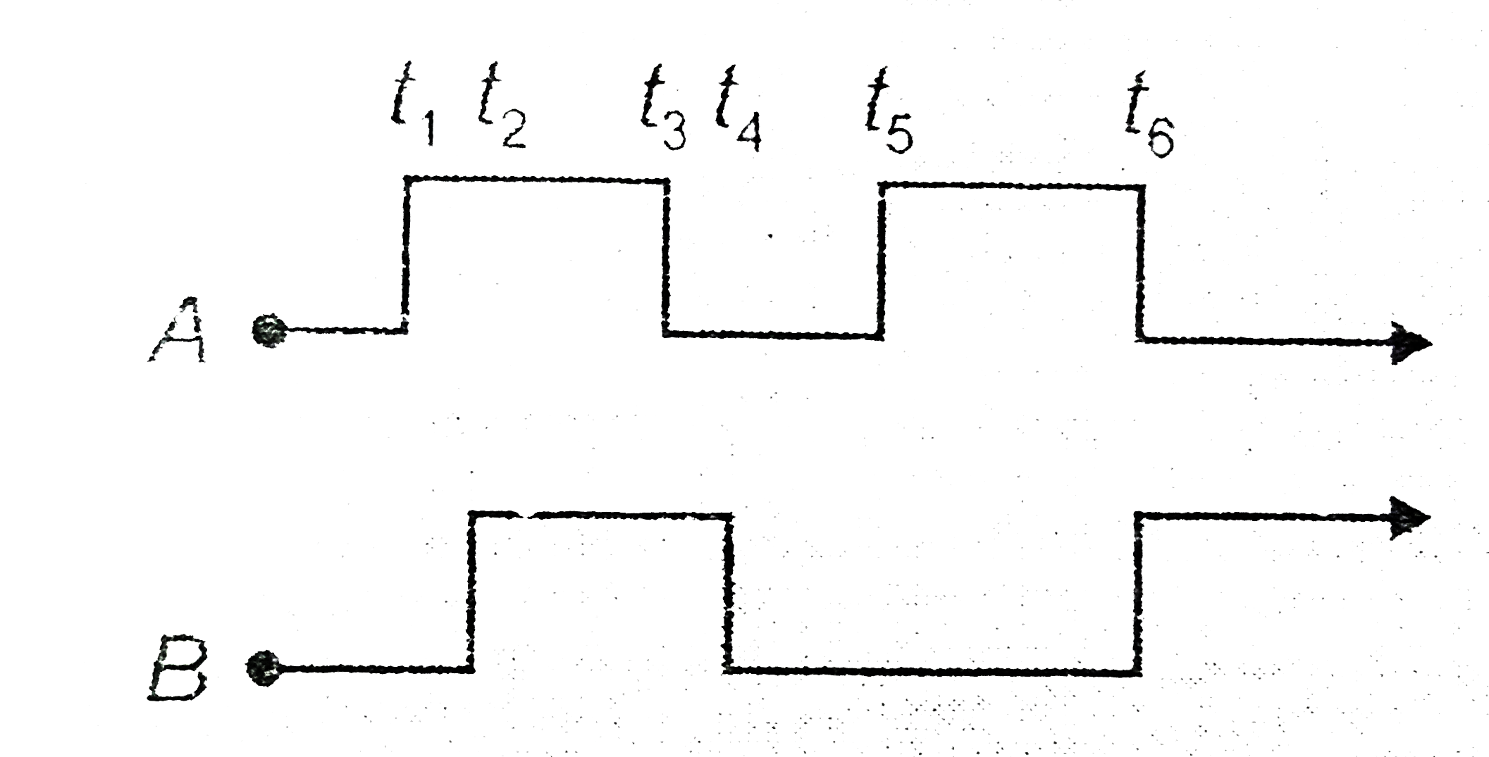
View SolutionShow the output waveform of OR gate for the following input waveforms of A and B

View Solutionshow the output waveform of AND gate for the following input waveforms of A and B.

View Solutionshow the output waveform of AND gate for the following input waveforms of A and B.

View SolutionThe output waveform of AND gate for the following input waveforms is
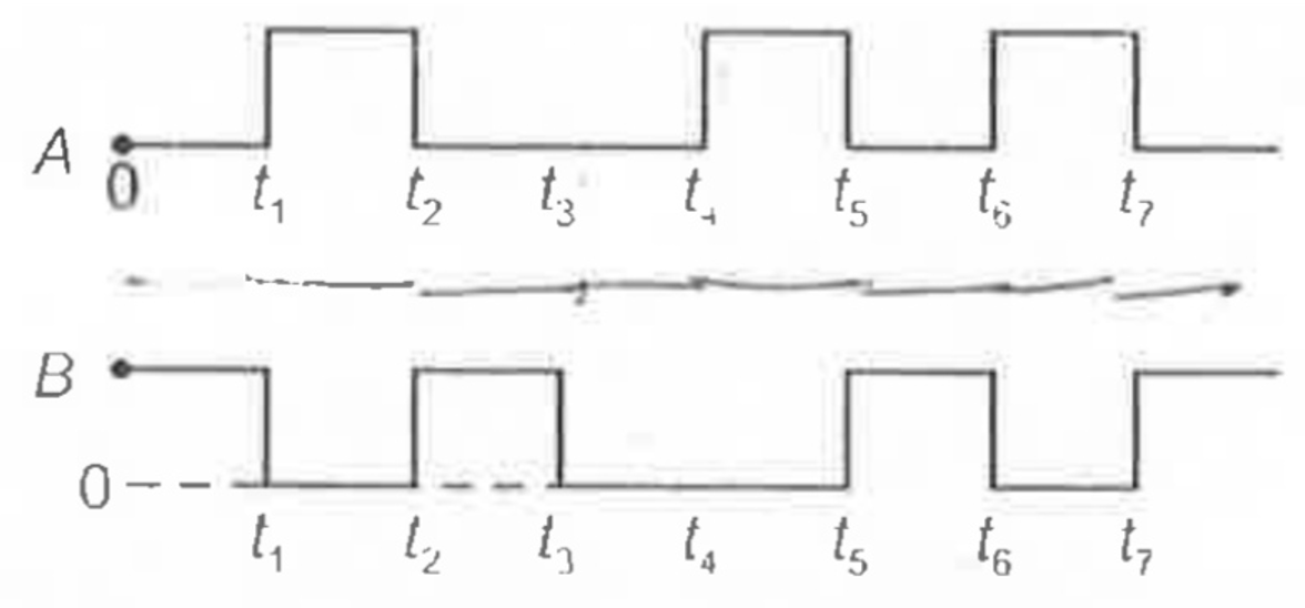
View Solution
