Draw the typical input and output characterisitics of an n-p-n transistor in CE configurtion . Show how these characteristic can be used to determine (a) the input resistance (r1) and (b) current amplification factor (β).
Characteristics of Transistor in C- E configuration:
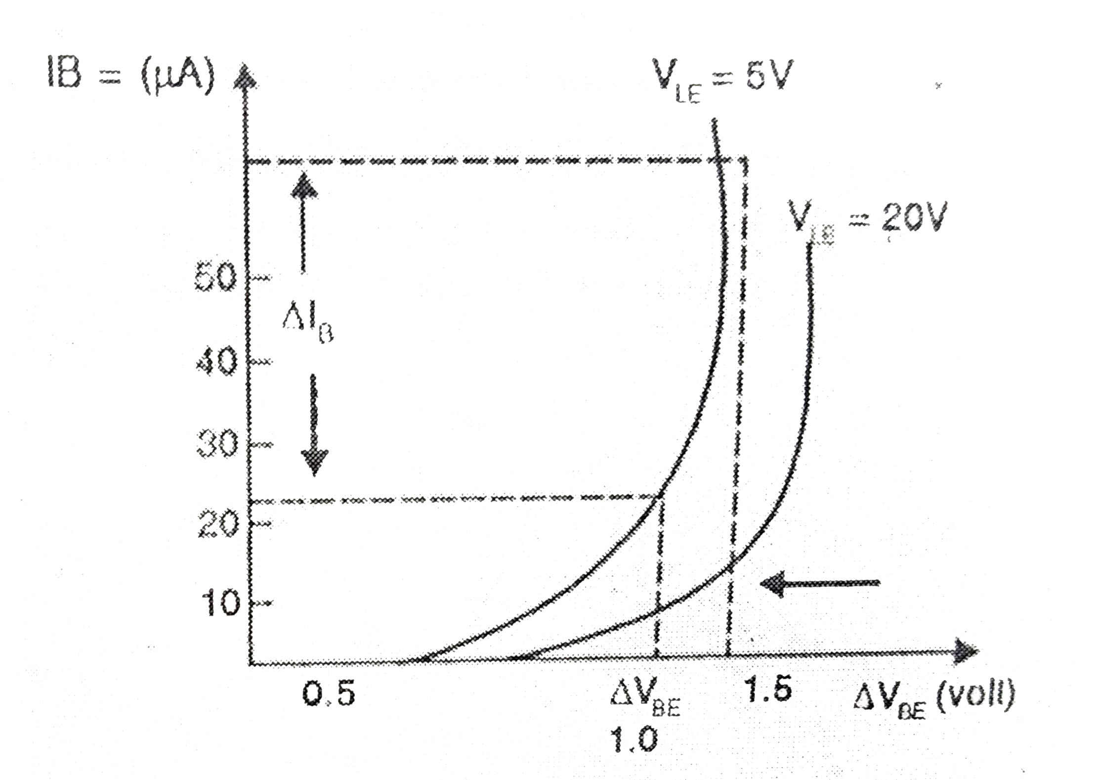
Input Characteristics: I/P ch in C - E configuration as shown. It is the curve between input current IB base current and the I/P voltage VBE (Bare Emitter voltage ) at constant callector emitter voltage (VLE)
Input Resistance : ri=ΔVBEΔIB∣VCE= constant
Dynamic I/P resistance ri is very small in CE configuration due to this after the cut in voltage base current IB increase rapidly with small increase on base-emitter volt. VBE
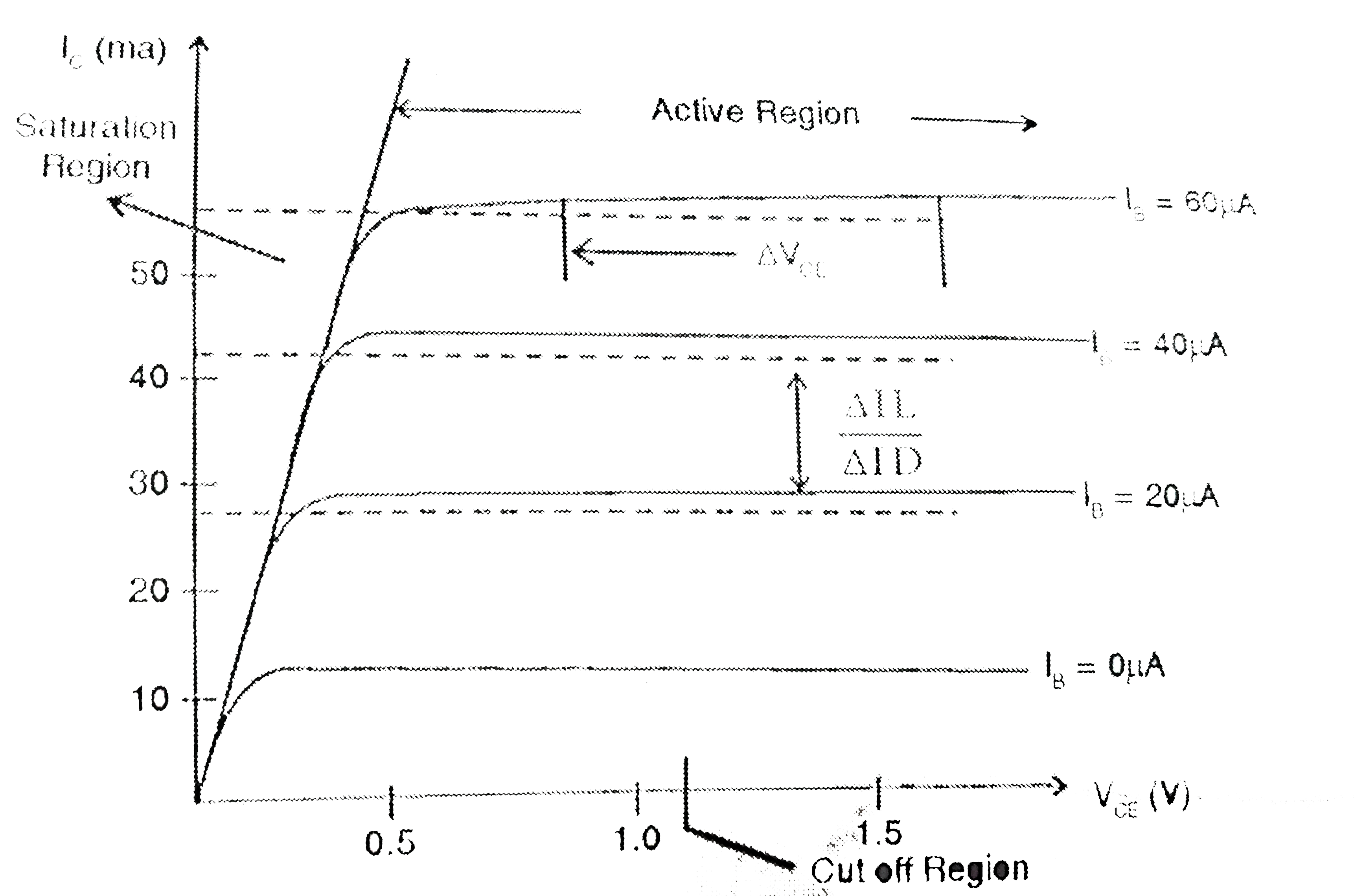
Output Characteristic: Output characetristic is a plate between the collector current IC and collector volt. VCB using base current IB as constant.
Bdc and Bac: We know that ,
Bdc=ICIB a.c Beta is obtained.
Bac=ΔICΔIB
Topper's Solved these Questions
- XII BOARDSBOOK - XII BOARDS PREVIOUS YEARCHAPTER - XII BOARDSEXERCISE - SECTION - A
7 Videos
- XII BOARDSBOOK - XII BOARDS PREVIOUS YEARCHAPTER - XII BOARDSEXERCISE - SECTION - B
9 Videos
- XII BOARDSBOOK - XII BOARDS PREVIOUS YEARCHAPTER - XII BOARDSEXERCISE - SECTION - E
6 Videos
- SAMPLE PAPER 2019BOOK - XII BOARDS PREVIOUS YEARCHAPTER - SAMPLE PAPER 2019EXERCISE - SECTION D
6 Videos
Similar Questions
Draw typical output characteristics of an n-p-n transistor in CE configuration. Show how these characteristics can be used to determine output resistance.
View Solution(a) Draw the circuit arrangement for studying the input and output characteristics of an n-p-n transistor in CE configuration . With the help of these characteristics define (i) input resistance , (ii) current amplification factor .
(b) Describe briefly with the help of a circuit diagram how an n-p-n transistor is used to produce self-sustained oscillations .
View Solution
Knowledge Check
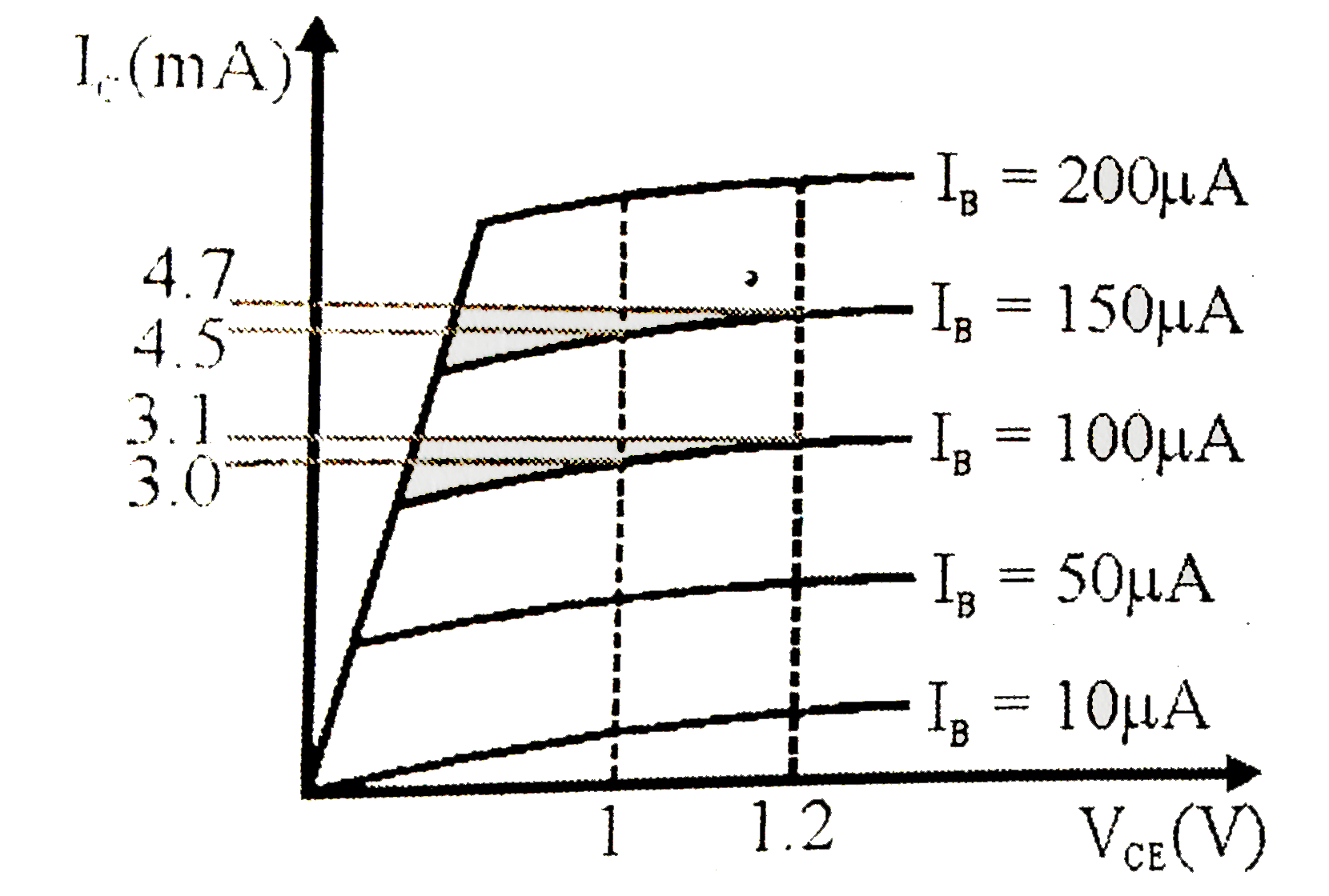
Output characteristic of n-p-n transistor in CE configuration is shown. From the characteristic curve determine the current gain at VCE=1V-A30B32C28D40
Draw a circuit diagram to study characteristics of n-p-n transistor in CE configuration. Draw the sketch of input and output characteristics of this configuration . Define current amplification factor ?
View SolutionDraw a circuit diagram to obtain the characteristics of a n-p-n transistor in common base configuration . Give shape of input and output characteristic curves.
View SolutionDraw the diagram of the circuit arangement used for studying the 'input' and the 'output' characteristics of an n-p-n transistor inits CE configuration. Briefly explain how these two types of characteristics are obtained and draw these characteristics.
(b) 'Define' the terms (i) Input resistance, (ii) Output resistance , (iii) Current amplification factor, for a given transistor.
View SolutionOutput characteristics of an n-p-n transistor in CE configuration is shown in the Fig. Determine
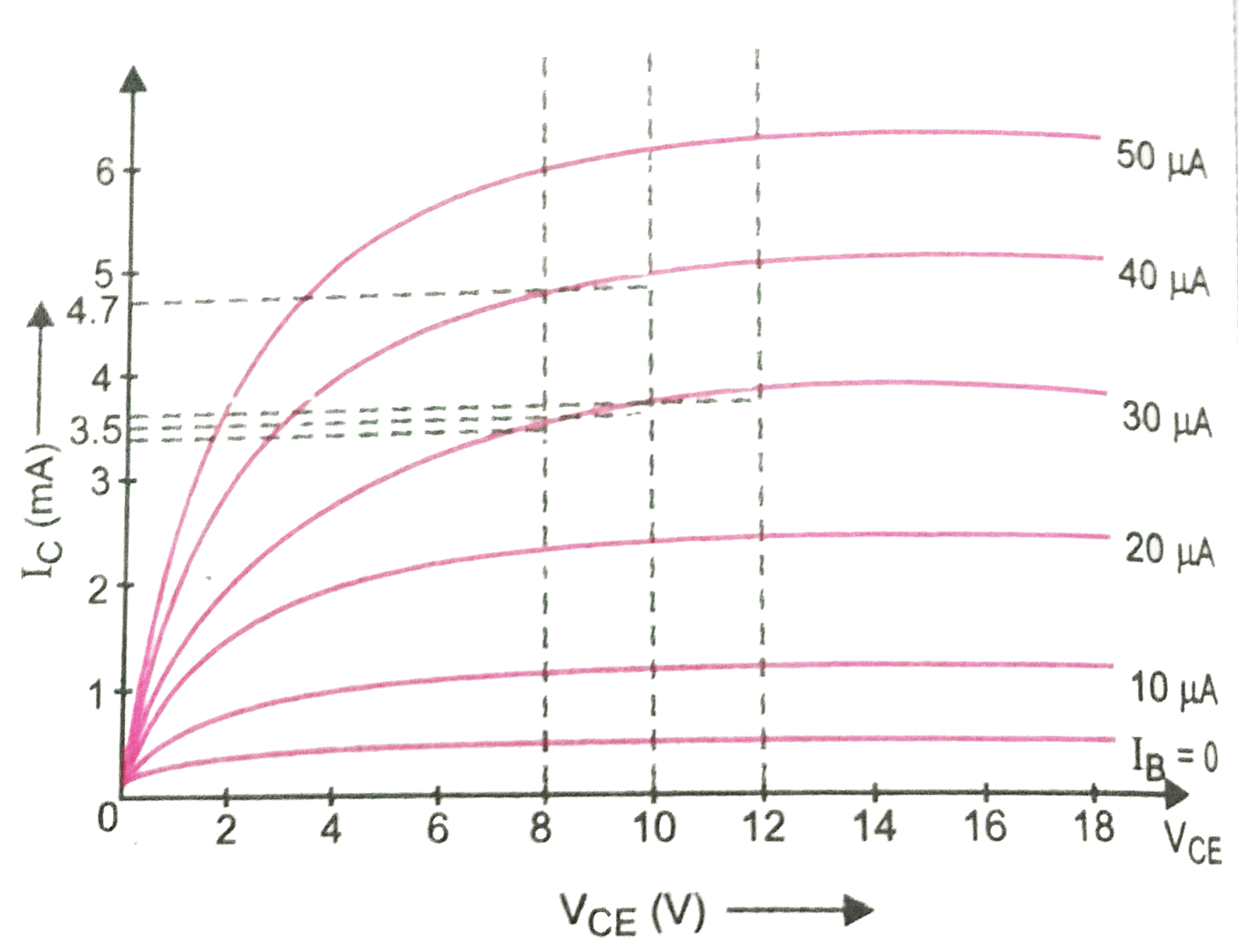
(i) dynamic output resistance (ii) dc current gain and (iii) ac current gain at an opererating point VCE=10V, when IB=30μA.
View SolutionOutput characteristics of an n-p-n transistor in CE configuration is shown in the Fig. Determine

(i) dynamic output resistance (ii) dc current gain and (iii) ac current gain at an opererating point VCE=10V, when IB=30μA.
View Solution(i) Draw a circuit diagram to study the input and output characteristics of an n-p-n transistor in its common emitter configuration. Draw the typical input and output characteristics.
(ii) Explain, with the hepl of a circuit diagram, the working of n-p-n transistor as a common emitter amplifier.
View SolutionDraw circuit diagram for n-p-n transistor to draw input and output characteristics in common base configuration. Draw the input and ouput curves and explain them.
View Solution
