(a) Students wants to use tow p-m jusnction diodes to convnet alternating current into direct current . Draw the labelled circuit she would use and explain how it works.
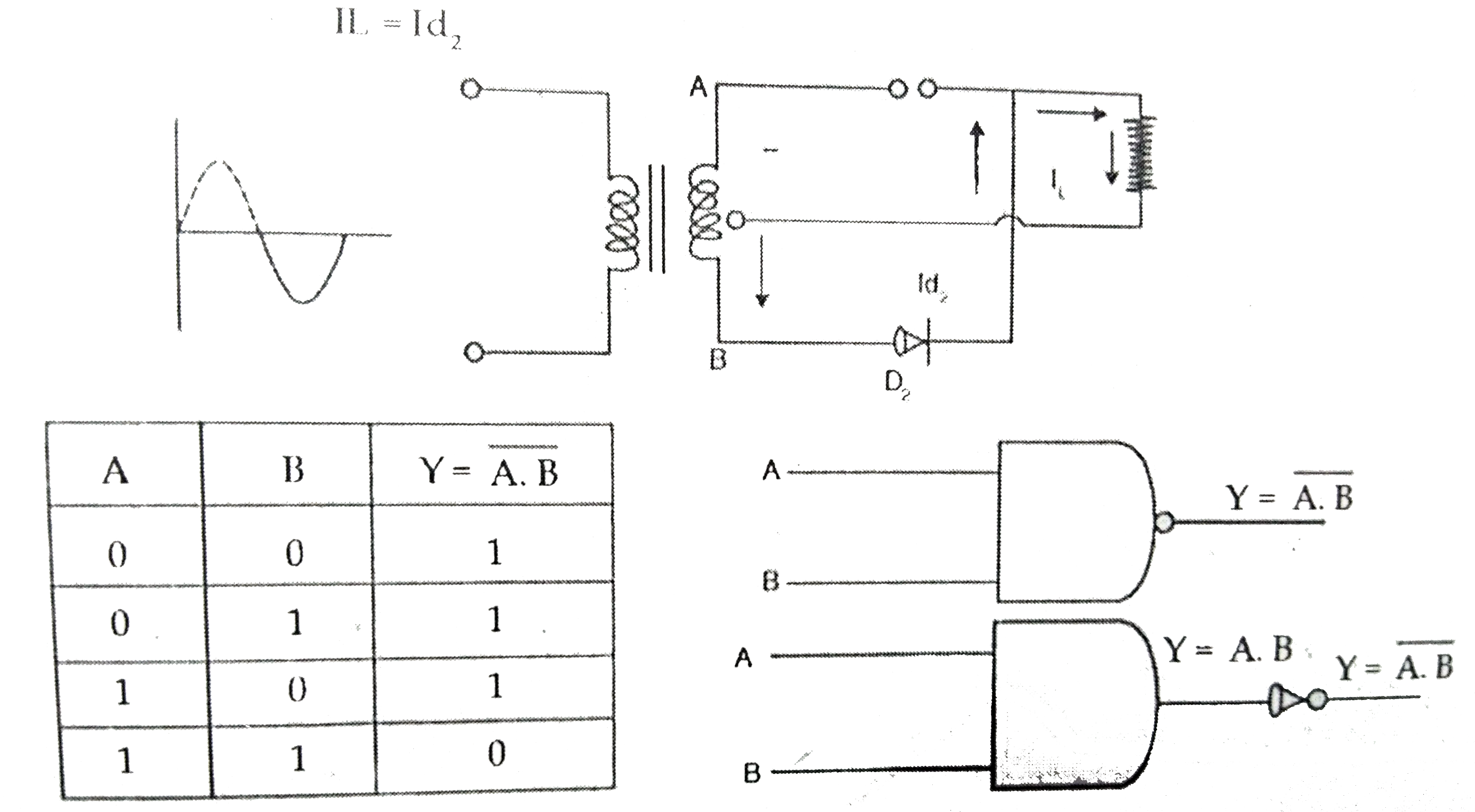
(b) Give the truth table and circuit symbol for NAND gate.
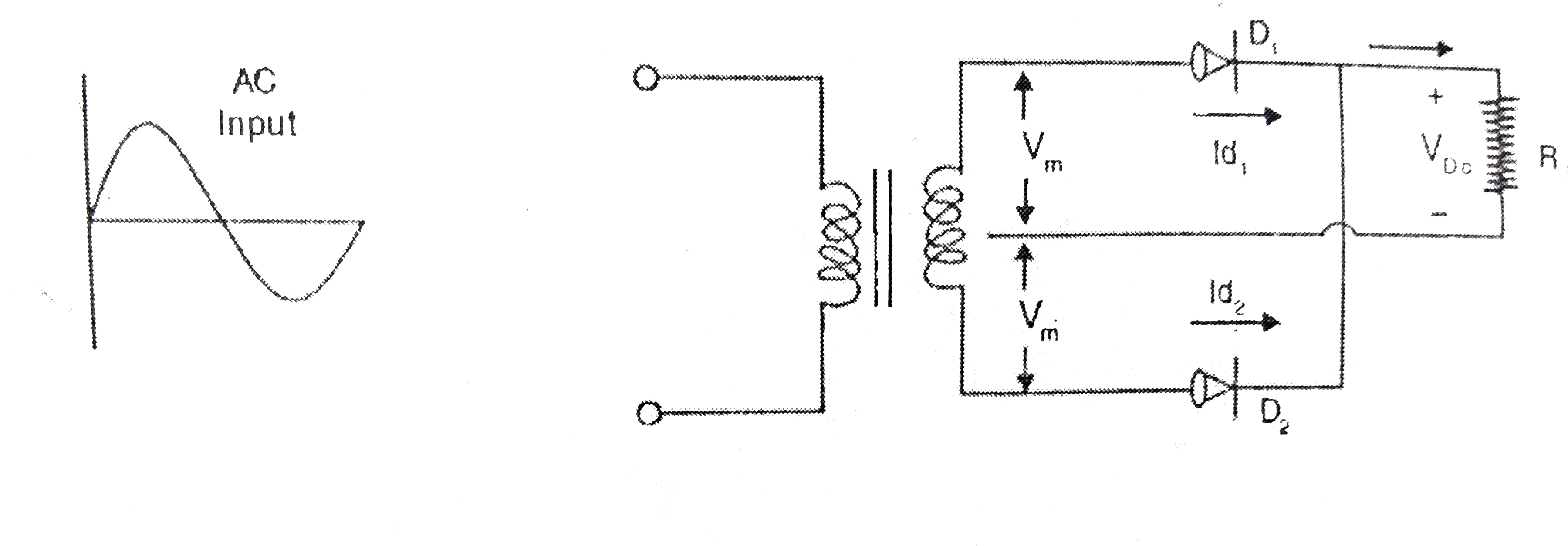
(a) To convert alternating current into direct current she should use full wave rectifier. The circuit diagra and working of full wave rectifier is as shown :

In this circuit there are two diodes in oder to rectify both the cycle of a . c I/P. For this centre tap transformer (ϕmer) is used .
(i) Operation during positive half cycle : During positive half cycle D1 diode is forward biasd and hence, wil conduct Id1 flows through RL. In this cycle diode. D2 is reverse baised and hence, does not conduct. Only D1 supplies the load current IL=IdI .

(ii) Operation during negative half-cycle : In the negavtive half cycle polarity reverse and A becomes- ve and B− becomes - ve and B− becomes +ve hence, the diode D1 does not conduct but D2 conducts being forwards biased current in the ciruit is as shown due to D2 .

Topper's Solved these Questions
- XII BOARDSBOOK - XII BOARDS PREVIOUS YEARCHAPTER - XII BOARDSEXERCISE - SECTION - A
7 Videos
- XII BOARDSBOOK - XII BOARDS PREVIOUS YEARCHAPTER - XII BOARDSEXERCISE - SECTION - B
9 Videos
- XII BOARDSBOOK - XII BOARDS PREVIOUS YEARCHAPTER - XII BOARDSEXERCISE - SECTION - E
6 Videos
- SAMPLE PAPER 2019BOOK - XII BOARDS PREVIOUS YEARCHAPTER - SAMPLE PAPER 2019EXERCISE - SECTION D
6 Videos
Similar Questions
(a) A student wants to use tow p-n junction diodes to convert alternating current in to direct curent draw the labelled circuit diagram she would use and explain how it works
(b) give the truth table and circuit symbol for NAND gate
View Solution(a) A student wants to use tow p-n junction diodes to convert alternating current in to direct curent draw the labelled circuit diagram she would use and explain how it works
(b) give the truth table and circuit symbol for NAND gate
View SolutionDrawa labelled diagram of a full-wave rectifier circuit and briefly explain its working, Show the input-output waveforms.
Or
A student wants to use two p-n junction diodes to convert a.c. into d.c. Draw the labelled circuit diagram she would use and explain how it works.
View Solution

(a) Draw the circuit diagram of reversed bias p-n junction.
(b). Draw the output wavefrom across diode in given circuit.
(c). Draw the truth table for the given logic gate.
View Solution

(a) Draw the circuit diagram of reversed bias p-n junction.
(b). Draw the output wavefrom across diode in given circuit.
(c). Draw the truth table for the given logic gate.
View SolutionIt is required to design a (two -input) logic gate, using an appropriate number, of :
(a) NAND gates that gives a 'low' output only when both the inputs are 'low'.
(b) NOR gates that gives a 'high' output only when both the inputs are 'high'.
Draw the logic circuits for these two cases and write the truth table, corresponding to each of the two designs.
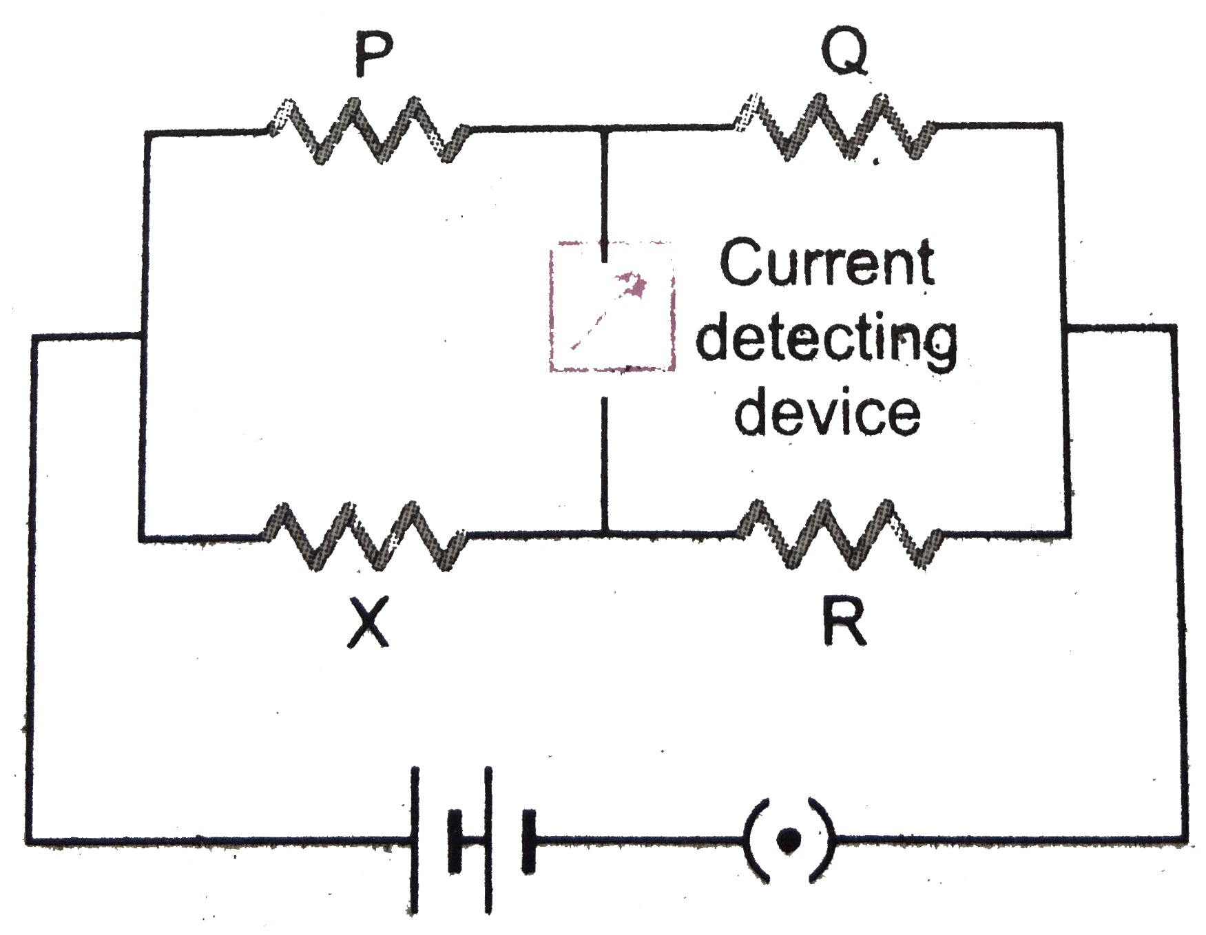
View Solution(a) Obtain the condition under which the current flowing in the current detecing device used in the circuit shown in figure, becomes zero.
(b) Describe briefly the device, based on the above condition. Draw a circuit diagram for this device and discuss, in brief, how it is used for finding as unknown resistance.

View SolutionUsing the wave forms of the input A and B, draw the output waveform of the given logic circuit . Identify the logic gate obtained . Write also the truth table.

View Solution
