
(a) Draw the circuit diagram of reversed bias p-n junction.
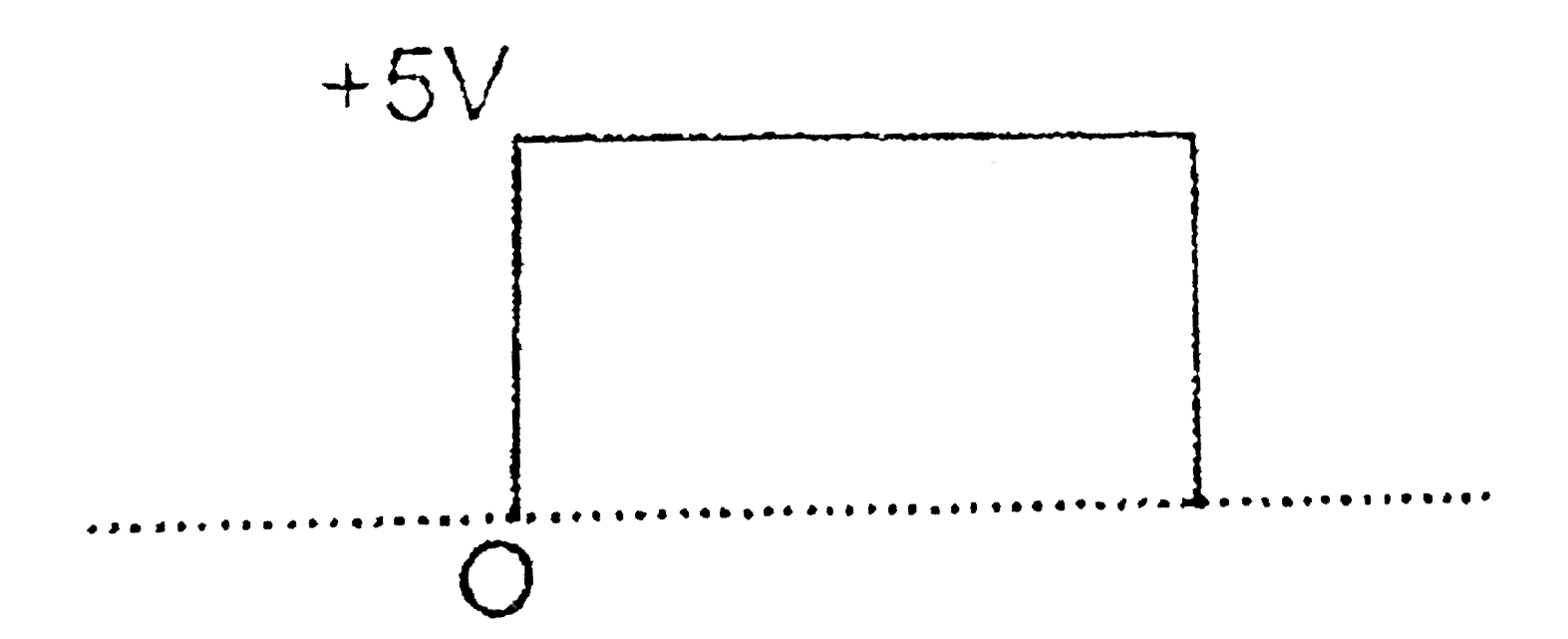
(b). Draw the output wavefrom across diode in given circuit.
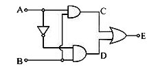
(c). Draw the truth table for the given logic gate.
Video Solution
Text Solution
(a). 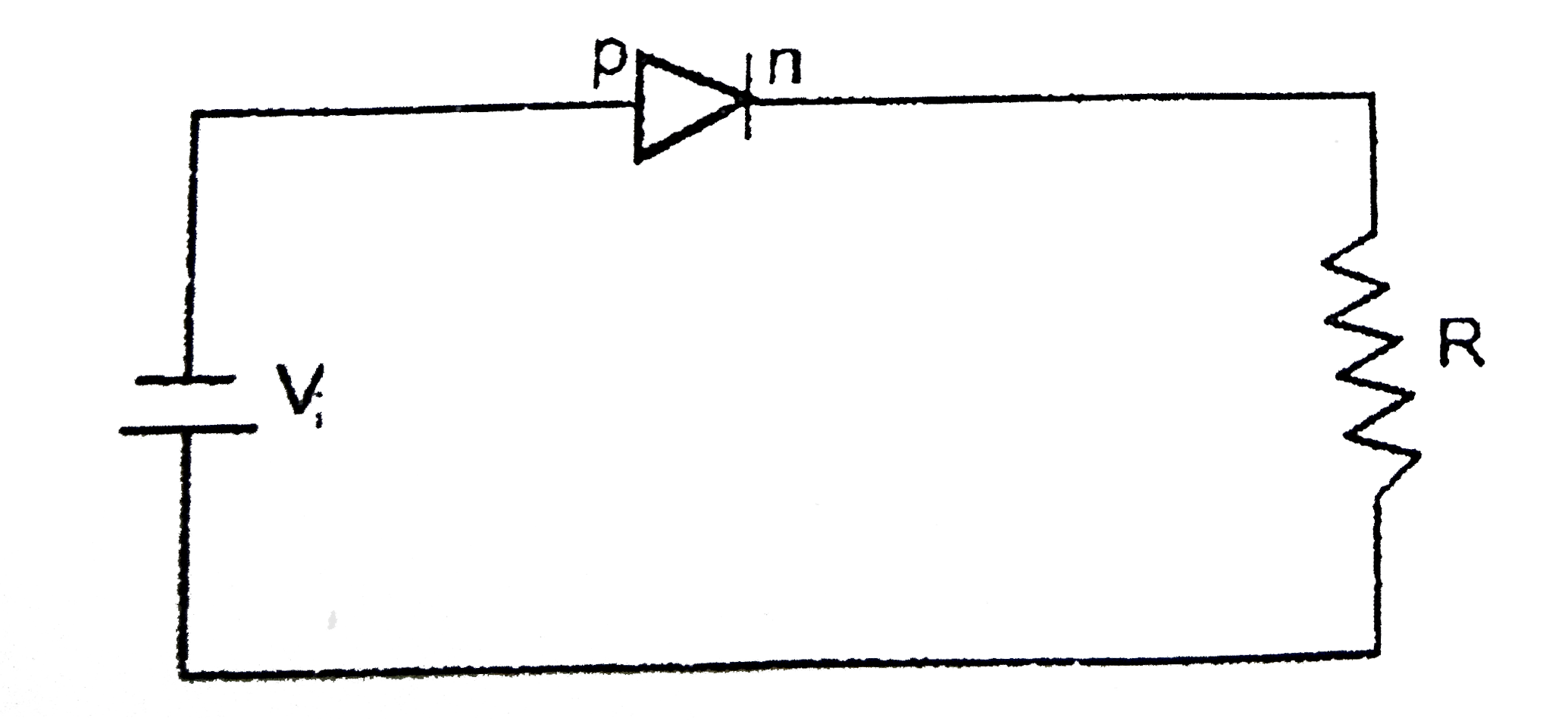
In reversed biased p-n junction positive terminal of the battery is connected to the n-side of diode and negative terminal of the battery is connected to p-side of diode.
(b). When input voltage is −5V the diode is reverse biased and no output is obtained. On the other hand when input is +5V the diode is forward biased and output is obtained which is +5V therefore,t he output wave from is shown in the figure.
(c) The given circuit is a combination of AND and NOT gate (NAND gate). The truth table will be as shown below:
ABA.BY=A.B1110010110010001
|
Updated on:21/07/2023
Topper's Solved these Questions
- BOOK - RESONANCE ENGLISHCHAPTER - SEMICONDUCTORSEXERCISE - Exercise 216videos
SEMICONDUCTORS
- BOOK - RESONANCE ENGLISHCHAPTER - REVISION DPPEXERCISE - All Questions463videos
REVISION DPP
- BOOK - RESONANCE ENGLISHCHAPTER - SIMPLE HARMONIC MOTION EXERCISE - Advanced Level Problems13videos
SIMPLE HARMONIC MOTION
Similar Questions
Knowledge Check
- Question 1 - Select One
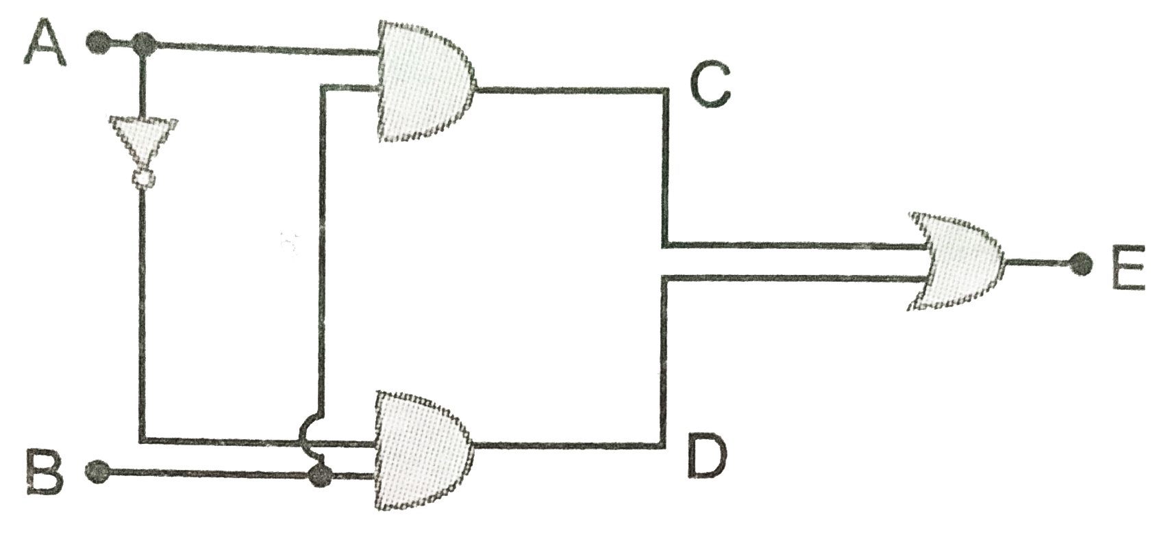
Truth table for the given circuit (Fig.)is
 A
A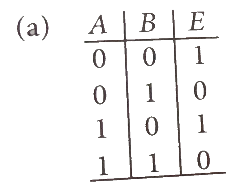 B
B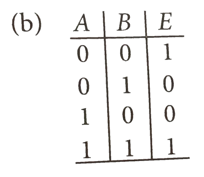 C
C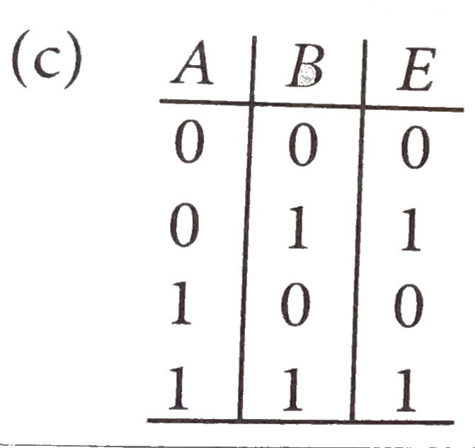 D
D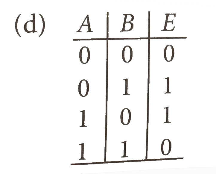
Truth table for the given circuit (Fig.)is
 View Solution
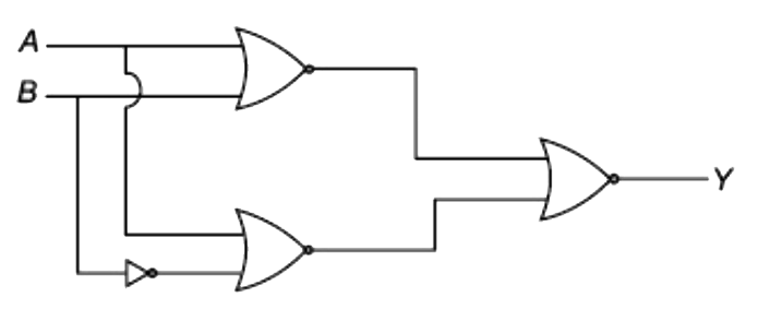
The output of the given logic circuit is
 View Solution
The truth table for the circuit given in the fig. isView SolutionDraw the circuit diagram of a half - wave rectifier using a p-n junction diode.
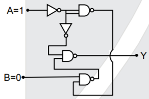
View SolutionOutput at terminal Y of given logic circuit.
 View Solution
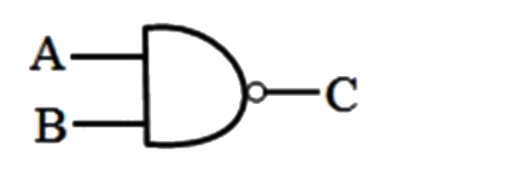
For given logic gate truth table is
 View Solution
Draw a labelled circuit diagram of a half wave rectifier and give its output waveform.
View Solution


