In a properly biased transistor-
both depletion layers are equially large.
both depletion layers are equally small.
Emitter-base depletion layer is large but base collector depletion layer is small.
Emitter-base depletion layer is small but base-collector depletion layer is large.
The correct Answer is:D
To solve the question regarding the depletion layer widths in a properly biased transistor, we can follow these steps:
Step 1: Understand the Transistor Configuration
A transistor consists of three regions: the emitter, the base, and the collector. In a properly biased transistor, the base-emitter junction is forward-biased, while the base-collector junction is reverse-biased.
Step 2: Analyze the Biasing Conditions
- Forward Bias (Base-Emitter Junction): When the base-emitter junction is forward-biased, it allows current to flow easily. This results in a smaller depletion region because the majority carriers (holes in the p-type base and electrons in the n-type emitter) are pushed towards the junction, reducing the width of the depletion layer.
- Reverse Bias (Base-Collector Junction): In contrast, when the base-collector junction is reverse-biased, it prevents current flow. This leads to a larger depletion region as the majority carriers are pulled away from the junction, widening the depletion layer.
Step 3: Compare the Depletion Layer Widths
- The depletion layer width at the base-emitter junction is small due to forward bias.
- The depletion layer width at the base-collector junction is large due to reverse bias.
Step 4: Conclusion
In a properly biased transistor:
- The depletion layer width at the base-emitter junction is small.
- The depletion layer width at the base-collector junction is large.
Thus, the correct answer is that the emitter-base depletion layer is small, while the base-collector depletion layer is large.
Final Answer
The depletion layer width in a properly biased transistor is small at the base-emitter junction and large at the base-collector junction.
---
A transistor consists of three regions: the emitter, the base, and the collector. In a properly biased transistor, the base-emitter junction is forward-biased, while the base-collector junction is reverse-biased.
- Forward Bias (Base-Emitter Junction): When the base-emitter junction is forward-biased, it allows current to flow easily. This results in a smaller depletion region because the majority carriers (holes in the p-type base and electrons in the n-type emitter) are pushed towards the junction, reducing the width of the depletion layer.
- Reverse Bias (Base-Collector Junction): In contrast, when the base-collector junction is reverse-biased, it prevents current flow. This leads to a larger depletion region as the majority carriers are pulled away from the junction, widening the depletion layer.
- The depletion layer width at the base-emitter junction is small due to forward bias.
- The depletion layer width at the base-collector junction is large due to reverse bias.
In a properly biased transistor:
- The depletion layer width at the base-emitter junction is small.
- The depletion layer width at the base-collector junction is large.
The depletion layer width in a properly biased transistor is small at the base-emitter junction and large at the base-collector junction.
Topper's Solved these Questions
- SEMICONDUCTORSBOOK - RESONANCE ENGLISHCHAPTER - SEMICONDUCTORSEXERCISE - Exercise 2
16 Videos
- SEMICONDUCTORSBOOK - RESONANCE ENGLISHCHAPTER - SEMICONDUCTORSEXERCISE - Exercise 3
88 Videos
- SEMICONDUCTORSBOOK - RESONANCE ENGLISHCHAPTER - SEMICONDUCTORSEXERCISE - Exercise 3
88 Videos
- REVISION DPPBOOK - RESONANCE ENGLISHCHAPTER - REVISION DPPEXERCISE - All Questions
463 Videos
- SIMPLE HARMONIC MOTION BOOK - RESONANCE ENGLISHCHAPTER - SIMPLE HARMONIC MOTION EXERCISE - Advanced Level Problems
13 Videos
Similar Questions
Knowledge Check
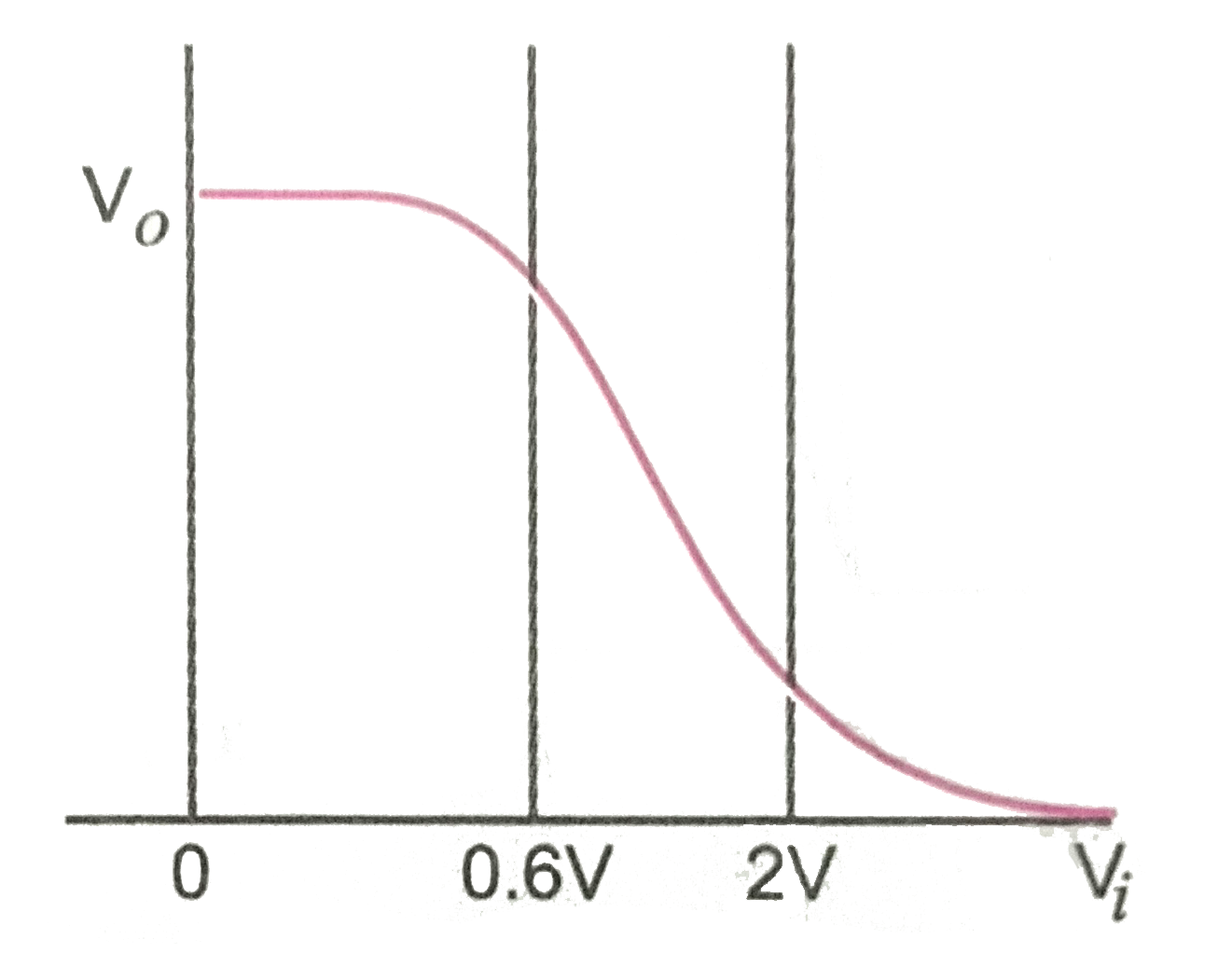
Fig.shows that transfer characteristics of a base biased CE transistor. Which of the following statements are true?
 AAt Vi=1V, it can be used as an amplifierBAt Vi=0.5V, it can be used as a switch turned offCAt Vi=2.5V, it can be used as a switch turned onDAll of these
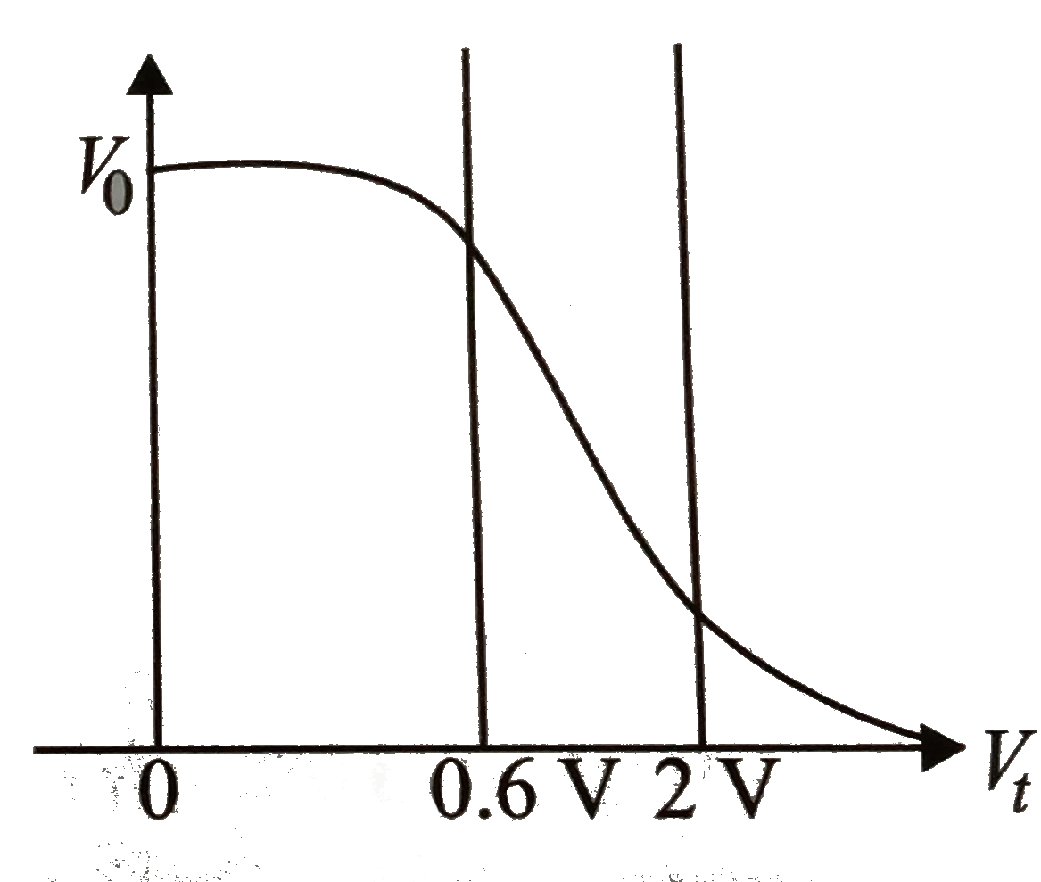
The transfer characteristics of a base biased common emitter transistor is shown in the figure. Which of the following statements are true?

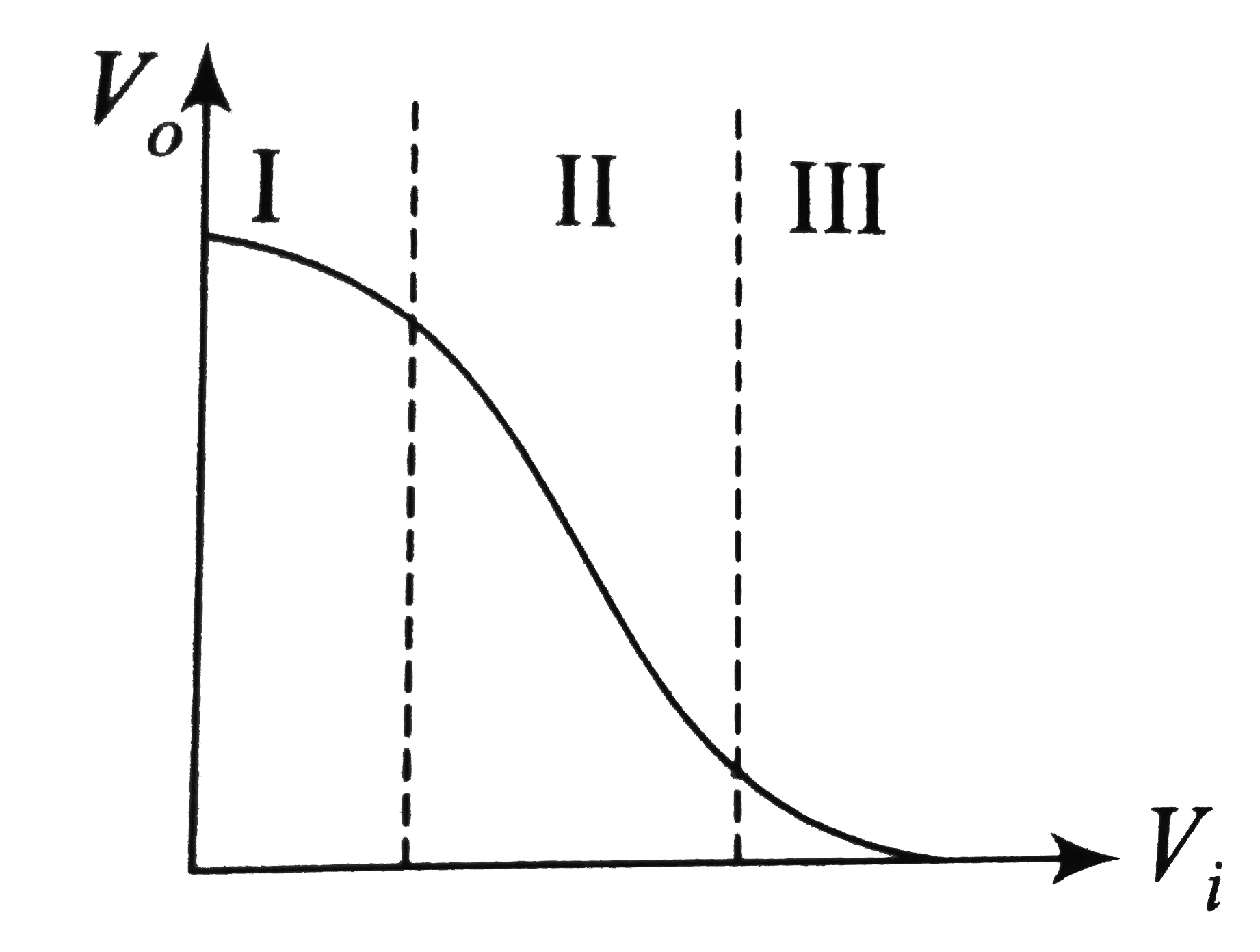
View SolutionTransfer characterstics [output voltage (Vo) vs. input voltage (Vi)] for a base biased transistor in CE configuration is as shown in the figure. For using transfor as a which, it is used

View SolutionIn a normal operation of a transistor,
(i) base-emitter junction is forward-biased
(ii) base-collector junction is forward-biased
(iii) base-emitter junction is reverse-baised
(iv) base-collector junction is reverse-biased
View SolutionDraw the tramsfer characteristic curve of a base biased transistor in CE configuration. Explain clearly how the active region of the Vo versus Vi curve in a transistor is used as an amplifier.
View SolutionIn a normal operation of a transistor,
View SolutionThe concentration of impurities in a transistor is
View SolutionIn a normal operation of a transistor,
View Solution
