In a p- n junction diode not connected to any circuit,
Potential is the same every where
The P-type side is at a higher potential than the N-type side
There is an electric field at the junction directed from the N-type side to the P-type side
There is an electric field at the junction directed from the P-type side to the N-type side
The correct Answer is:C
To solve the question regarding the behavior of a p-n junction diode not connected to any circuit, we can break it down into the following steps:
1. Understanding the Structure of a p-n Junction Diode:
- A p-n junction diode consists of two types of semiconductor materials: p-type and n-type. The p-type semiconductor has an abundance of holes (positive charge carriers), while the n-type semiconductor has an abundance of electrons (negative charge carriers).
2. Formation of the Depletion Region:
- When a p-n junction is formed, electrons from the n-type region will diffuse into the p-type region and recombine with holes. Similarly, holes from the p-type region will diffuse into the n-type region and recombine with electrons.
- This movement of charge carriers leads to the formation of a depletion region at the junction, where there are no free charge carriers (electrons or holes).
3. Electric Field Creation:
- As electrons leave the n-type region and recombine with holes in the p-type region, the n-type side becomes positively charged (due to the ionized donor atoms), and the p-type side becomes negatively charged (due to the ionized acceptor atoms).
- This separation of charge creates an electric field in the depletion region.
4. Direction of the Electric Field:
- The electric field in the depletion region is directed from the n-type region to the p-type region. This is because the positive charge (from the n-type) is on the side of the n-type material and the negative charge (from the p-type) is on the side of the p-type material.
5. Conclusion:
- Therefore, in a p-n junction diode that is not connected to any circuit, an electric field is established in the depletion region, directed from the n-side to the p-side.
Final Answer:
- The electric field in the depletion region of a p-n junction diode not connected to any circuit is directed from the n-type side to the p-type side.
- A p-n junction diode consists of two types of semiconductor materials: p-type and n-type. The p-type semiconductor has an abundance of holes (positive charge carriers), while the n-type semiconductor has an abundance of electrons (negative charge carriers).
- When a p-n junction is formed, electrons from the n-type region will diffuse into the p-type region and recombine with holes. Similarly, holes from the p-type region will diffuse into the n-type region and recombine with electrons.
- This movement of charge carriers leads to the formation of a depletion region at the junction, where there are no free charge carriers (electrons or holes).
- As electrons leave the n-type region and recombine with holes in the p-type region, the n-type side becomes positively charged (due to the ionized donor atoms), and the p-type side becomes negatively charged (due to the ionized acceptor atoms).
- This separation of charge creates an electric field in the depletion region.
- The electric field in the depletion region is directed from the n-type region to the p-type region. This is because the positive charge (from the n-type) is on the side of the n-type material and the negative charge (from the p-type) is on the side of the p-type material.
- Therefore, in a p-n junction diode that is not connected to any circuit, an electric field is established in the depletion region, directed from the n-side to the p-side.
- The electric field in the depletion region of a p-n junction diode not connected to any circuit is directed from the n-type side to the p-type side.
Topper's Solved these Questions
- BOOK - RESONANCE ENGLISHCHAPTER - SEMICONDUCTORSEXERCISE - Exercise 216videos
SEMICONDUCTORS
- BOOK - RESONANCE ENGLISHCHAPTER - REVISION DPPEXERCISE - All Questions463videos
REVISION DPP
- BOOK - RESONANCE ENGLISHCHAPTER - SIMPLE HARMONIC MOTION EXERCISE - Advanced Level Problems13videos
SIMPLE HARMONIC MOTION
Similar Questions
Knowledge Check
- Question 1 - Select One
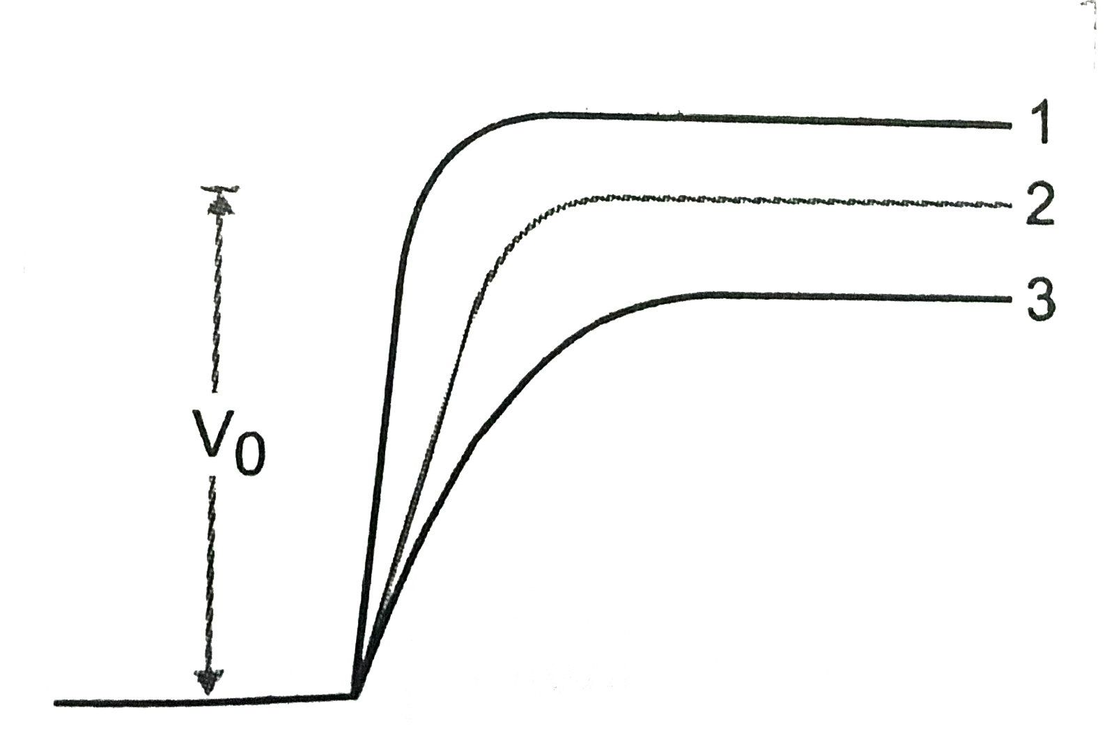
In Fig . V0 is the potential barrier across a p-n junction, when no battery is connected across the junction
 A1 and 3 both correspond to forward bias of junctionB3 corresponds to forward bias of junction and 1 corresponds to reverse bias of junctionC1 corresponds to forward bias and 3 corresponds to reverse bias of junction.D3 and 1 both correspond to reverse bias of junction.
In a p-n junction with open ends,
View SolutionIn a p-n junction with open ends,
View SolutionAssertion: In reverse biased condition a p-n junction diode does not conduct.
Reason: In reverse biased condition a diode has zero resistance.View SolutionIn junction diode, the holes are due to
View SolutionBarrier potential of a p−n junction diode does not depend on
View SolutionBarrier potential of a p−n junction diode does not depend on
View SolutionIn Fig . V0 is the potential barrier across a p-n junction, when no battery is connected across the junction
 View Solution

