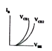
Input characteristics are shown for CE configuration of n-p-n transistor for different output voltage. Here.

A) VCE1>VCE2
B) VCE1
C) VCE1<VCE2
D) none of these
The correct Answer is:A
Step by step video & image solution for Input characteristics are shown for CE configuration of n-p-n transistor for different output voltage. Here. by Physics experts to help you in doubts & scoring excellent marks in Class 12 exams.
Updated on:21/07/2023Topper's Solved these Questions
- PRACTICAL PHYSICSBOOK - AAKASH SERIESCHAPTER - PRACTICAL PHYSICSEXERCISE - LECTURE SHEET LEVEL-II (ADVANCED) Linked Comprehension Type Questions
4 Videos
- PRACTICAL PHYSICSBOOK - AAKASH SERIESCHAPTER - PRACTICAL PHYSICSEXERCISE - LECTURE SHEET LEVEL-II (ADVANCED) Linked Comprehension Type Questions
4 Videos
- PHYSICAL WORLDBOOK - AAKASH SERIESCHAPTER - PHYSICAL WORLDEXERCISE - Exercise -I
10 Videos
- RAY OPTICSBOOK - AAKASH SERIESCHAPTER - RAY OPTICSEXERCISE - PROBLEMS ( LEVEL-II)
60 Videos
Similar Questions
A n−p−n transistor conducts when
View SolutionThe symbol of p-n-p transistor is
View SolutionThe number of terminals in n−p−n transistor is
View SolutionDescribe briefly the functions of the three segments of n-p-n transistor.
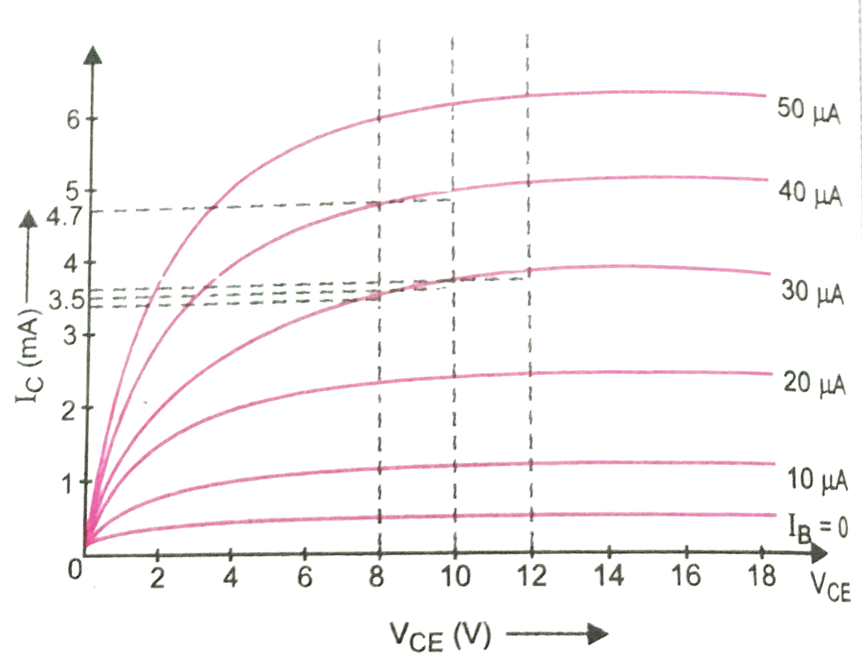
View SolutionOutput characteristics of an n-p-n transistor in CE configuration is shown in the Fig. Determine

(i) dynamic output resistance (ii) dc current gain and (iii) ac current gain at an opererating point VCE=10V, when IB=30μA.
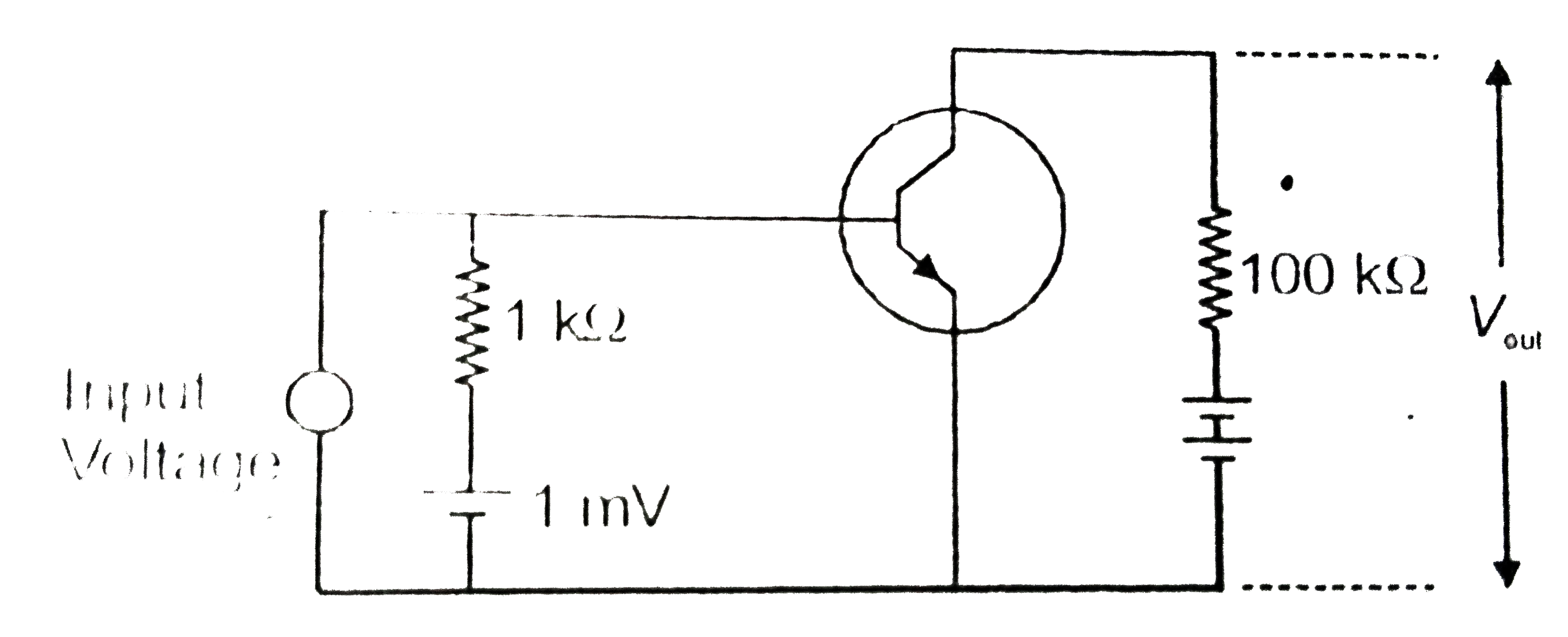
View SolutionIn the following common emitter configuration an n-p-n transistor with current gain β=100 is used. What is the output voltage of the amplifier ?

View SolutionDraw typical output characteristics of an n-p-n transistor in CE configuration. Show how these characteristics can be used to determine output resistance.
View SolutionDraw the diagram of the circuit arangement used for studying the 'input' and the 'output' characteristics of an n-p-n transistor inits CE configuration. Briefly explain how these two types of characteristics are obtained and draw these characteristics.
(b) 'Define' the terms (i) Input resistance, (ii) Output resistance , (iii) Current amplification factor, for a given transistor.
View Solution(i) Draw a circuit diagram to study the input and output characteristics of an n-p-n transistor in its common emitter configuration. Draw the typical input and output characteristics.
(ii) Explain, with the hepl of a circuit diagram, the working of n-p-n transistor as a common emitter amplifier.
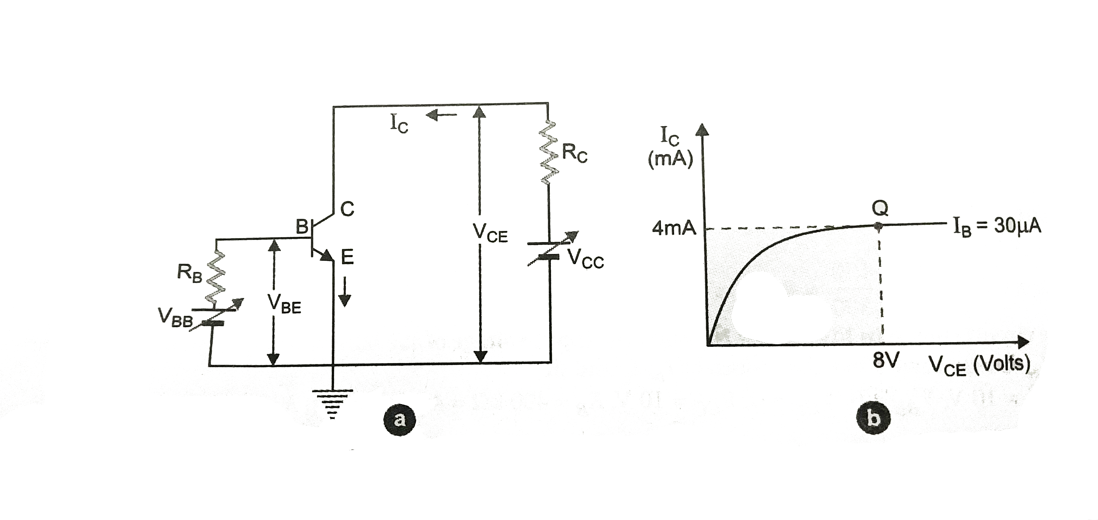
View SolutionConsider the circuit arrangnent shown in Fig. for studying input and output characteristics of npn transistor in CE configuration.
Select the values of R and R for a transistor whose VBE=0.7V, so that the transistor is operating at point Q as shown in the characteristics shown in Fig.
 Given that the input impedance of the transistor is very small and VCC=VBB=16V, also find the voltage gain and power gain of circuit making appropriate assumptions.
View Solution
