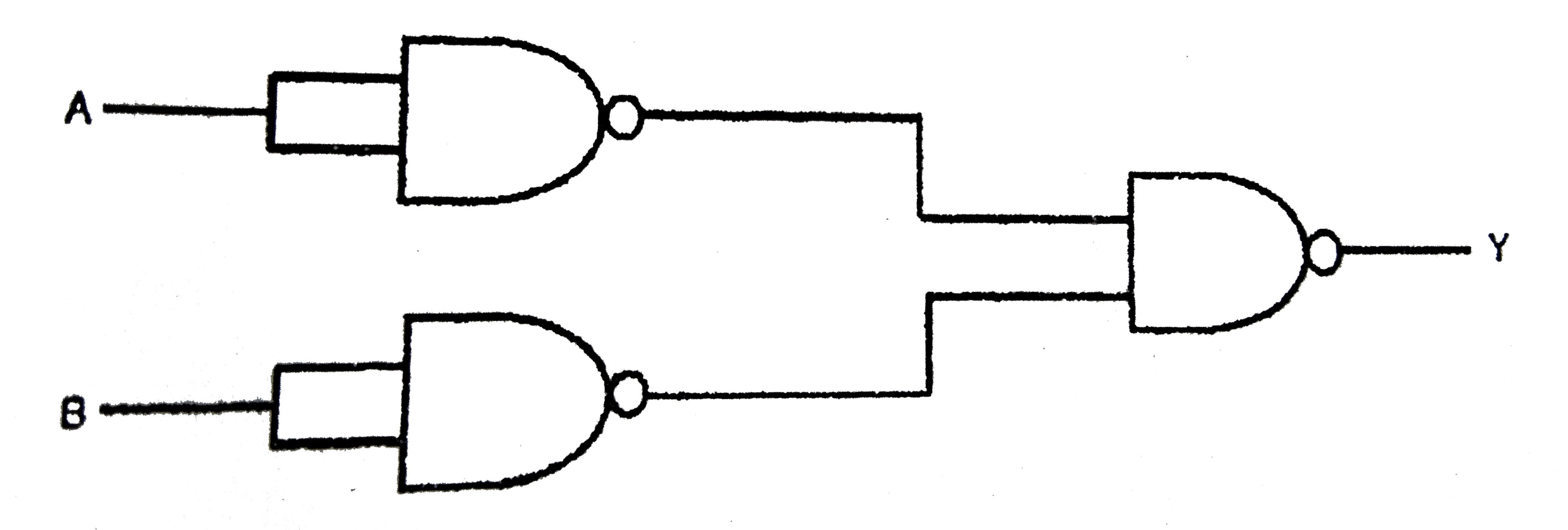
Identity the equivalent gate represented by the circuit shown in the figure. Draw its logic symbol and write the truth table.

Or Gate 
Topper's Solved these Questions
- BOOK - OSWAAL PUBLICATIONCHAPTER - SEMI-CONDUCTORS ELECTRONICSEXERCISE - TOPIC -4 LOGIC GATES (SHORT ANSWER TYPE QUESTIONS-II)2videos
SEMI-CONDUCTORS ELECTRONICS
- BOOK - OSWAAL PUBLICATIONCHAPTER - SEMI-CONDUCTORS ELECTRONICSEXERCISE - TOPIC -4 LOGIC GATES (NUMERICAL PROBLEMS)4videos
SEMI-CONDUCTORS ELECTRONICS
- BOOK - OSWAAL PUBLICATIONCHAPTER - SEMI-CONDUCTORS ELECTRONICSEXERCISE - TOPIC -4 LOGIC GATES (VERY SHORT ANSWER TYPE QUESTIONS)3videos
SEMI-CONDUCTORS ELECTRONICS
- BOOK - OSWAAL PUBLICATIONCHAPTER - Sample Paper 8EXERCISE - Exercise37videos
Sample Paper 8
- BOOK - OSWAAL PUBLICATIONCHAPTER - SOLVED PAPER (II PUC JULY 2016)EXERCISE - PART D11videos
SOLVED PAPER (II PUC JULY 2016)
Similar Questions

Name of gate obtained from the combination of gates shown in the figure. Draw its logic symbol. Write the truth table of the combination.View Solution
Name of gate obtained from the combination of gates shown in the figure. Draw its logic symbol. Write the truth table of the combination.View SolutionDraw the symbol for AND gate and write its truth table.
 View Solution
Draw the logic symbol of NAND gate and give its Truth table
View SolutionGive logic symbol and truth table for a NOT gate.
View SolutionDraw symbol and truth table for AND gate .
View Solution(a) In the figure given below the input waveform is converted into the output waveform by a device 'X'. Name the device and draw its circuit diagram.

(b) Identify the logic gate represented by the circuit as shown and write its truth table.
 View Solution
Draw the truth table for the logic gate arrangement shown in the figure.View Solution
Draw the truth table for the logic gate arrangement shown in the figure.View SolutionDraw the symbol and truth table of OR gate.
View Solution
