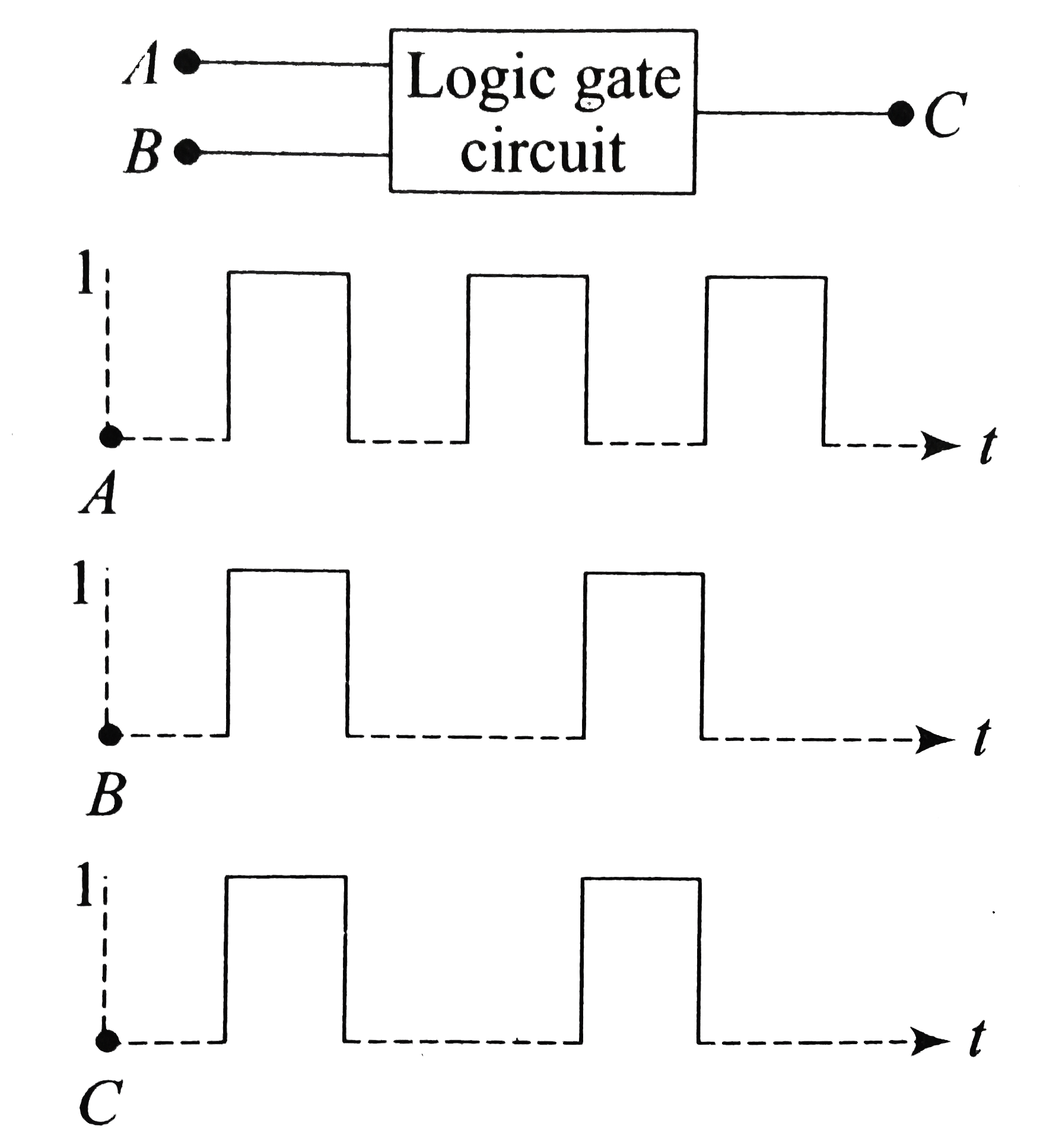
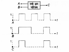
The following figure shows a logic gate circuit with two inputs A and B output C. The voltage waveforms of A,B and C are as shown in second figure given below :-
_E01_436_Q01.png)
The logic circuit gate is :-Solution in Gujrati
OR gate
AND gate
NAND gate
NOR gate
The correct Answer is:B
Step by step video & image solution for The following figure shows a logic gate circuit with two inputs A and B output C. The voltage waveforms of A,B and C are as shown in second figure given below :- The logic circuit gate is :- by Physics experts to help you in doubts & scoring excellent marks in Class 11 exams.
Updated on:21/07/2023Topper's Solved these Questions
- SEMICONDUCTORSBook:ALLEN Chapter:SEMICONDUCTORSExercise:Part-3(Exercise-3)
Explore 27 Videos
- SEMICONDUCTORSBook:ALLEN Chapter:SEMICONDUCTORSExercise:Part-3(Exercise-4)
Explore 50 Videos
- SEMICONDUCTORSBook:ALLEN Chapter:SEMICONDUCTORSExercise:Part-3(Exercise-1)
Explore 84 Videos
- PHYSICAL WORLD, UNITS AND DIMENSIONS & ERRORS IN MEASUREMENT Book:ALLEN Chapter:PHYSICAL WORLD, UNITS AND DIMENSIONS & ERRORS IN MEASUREMENT Exercise:EXERCISE-IV
Explore 7 Videos
- WAVES AND OSCILLATIONSBook:ALLEN Chapter:WAVES AND OSCILLATIONSExercise:Part-1(Exercise-05)[B]
Explore 42 Videos
Similar Questions
Assertion: Microwave communication is preferred to optical communication
Reason: Microwaves provide large number of channels and bandwidths as compared to optical signals.
View SolutionAt absolute zero temperature Si acts as ……..
View SolutionIn semiconductor the valence band at 0 K is
View SolutionAssertion : Gravitational forces do not depend on the medium between the masses.
Reason : Mediating particle responsible for gravitational force is graviton.
View SolutionA string of length 0.4m and mass 10−2kg is clamped at one end . The tension in the string is 1.6N. The identical wave pulses are generated at the free end after regular interval of time , Δt . The minimum value of Δt , so that a constructive interference takes place between successive pulses is
View SolutionThe following figure shows a logic gate circuit with two inputs A and B and the output C. The voltage waveforms of A,B and C are as shown below
View SolutionThe following figure shows a logic gate circuit with two inputs A and B output C. The voltage waveforms of A,B and C are as shown in second figure given below :-
_E01_436_Q01.png)
The logic circuit gate is :-
View SolutionThe following figure shows a logic gate circuit with two inputs A and B and the output Y. The voltage waveforms of A,B and Y are as given : The logic gate is
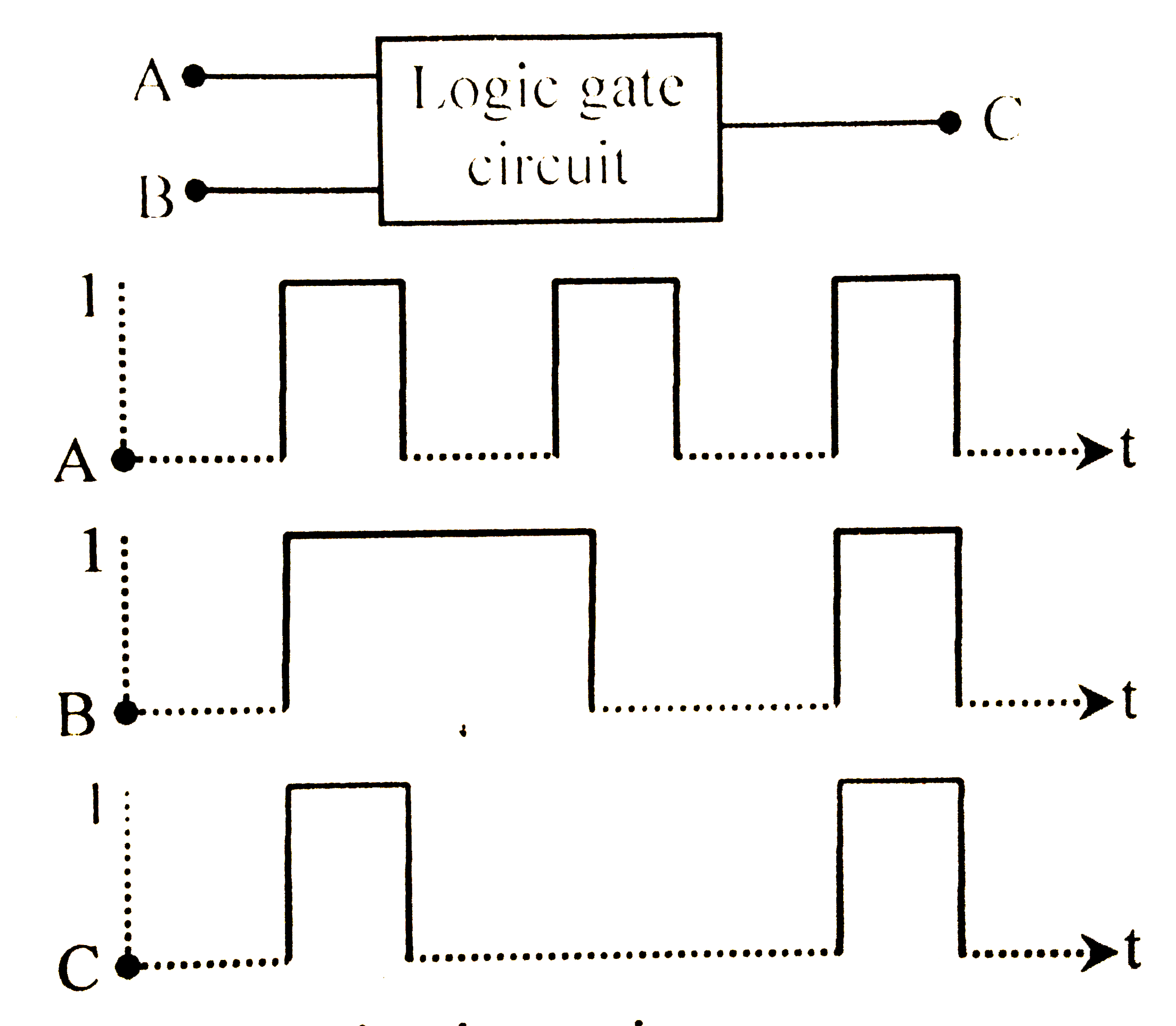
View SolutionThe following figure shows a logic gate circuit with two inputs A and B and the output C. The voltage waveforms of A, B and C are as shown below-
View SolutionThe following figure shows a logic gate circuit with two inputs A and B and the output C. The voltage waveforms of A, B and C are as shown below.
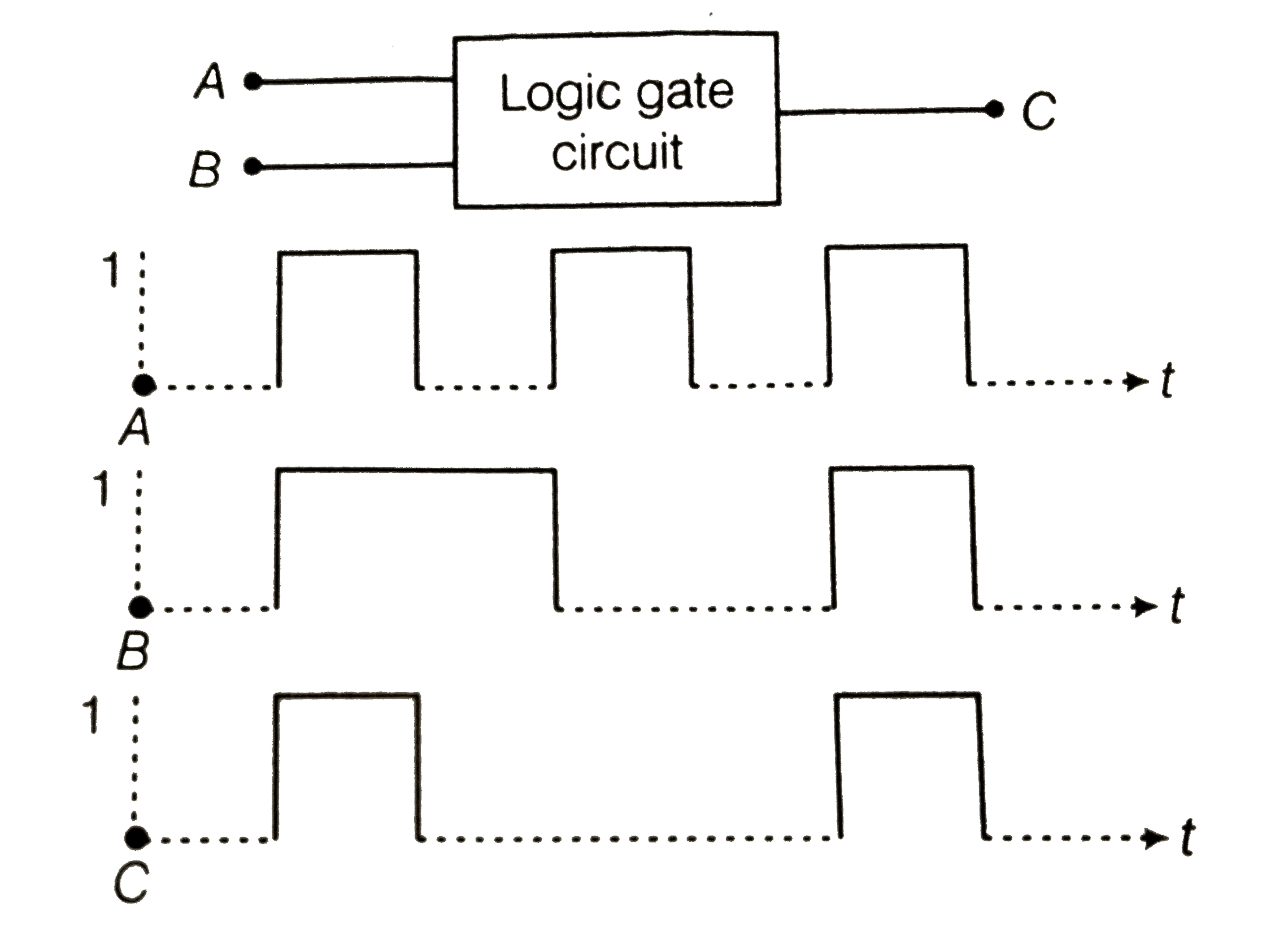
The logic circuit gate is
View SolutionThe following figure showns a AND logic gate circuit with two inputs A and B and the output C. The voltage waveforms at C will be -
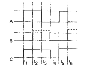
View Solutionचित्र में एक लॉजिक परिपथ में दो निवेशी A तथा B और एक निर्गत C दर्शाया गया है| A,B तथा C के वोलटता तरंगरूप दिए गए अनुसार है| तब लॉजिक परिपथ गेट है-
View SolutionThe following figure shown a logic gate circuit with ttwo inputs A and B and the C are as shown below The logic circuit gate is
View Solutionनिम्नलिखित चित्र में एक तर्क द्वार परिपथ को दिखाया गया है जिसमें दो निवेश A और B और एक निर्गत हैं। A,B और C के वोल्टता तरंग-रूप निम्न प्रकार हैं
यह तर्क परिपथ द्वार है
View SolutionThe following shows a logic gate circuit with two inputs A and B and the output C. The voltage waveforms of A, B and C are as shown below.
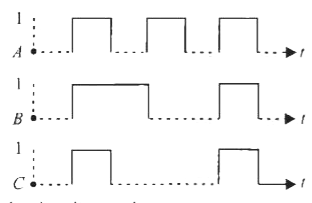
The logic circuit gate is
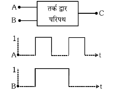
View Solutionनिम्नलिखित चित्र में एक AND तर्क द्वार परिपथ को दिखाया गया है जिसमें दो निवेश A और B और एक निर्गत C हैं। C की वोल्टता का तरंग-रूप निम्न प्रकार होगा
View Solution
