Complete Solutions to Section-B : Numericals (Numerical From .DARPAN. Based On Textbook) of chapter SEMICONDUCTOR ELECTRONICS : MATERIALS, DEVICES AND SIMPLE CIRCUITS of Class 12 book with complete answers and questions
| Class 12 | PHYSICS |
| Chapter | SEMICONDUCTOR ELECTRONICS : MATERIALS, DEVICES AND SIMPLE CIRCUITS |
| KUMAR PRAKASHAN | Section-B : Numericals (Numerical From .DARPAN. Based On Textbook) |
| Number Of Questions | 14 |
| Academic Year | 2023-24 |
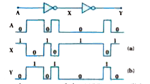
A logic circuit is shown in the diagram. Draw the output signal at the point X and Y for the input signal shown in the figure at point A.
View SolutionPrepare the truth table for the logic circuit given below.

View SolutionWhich gate will be obtained by joining the two inputs of the NAND gate?
View SolutionShow that the circuit drawn in the figure comprising of 3 NAND gate behaves as an OR gate.
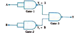
View SolutionGive truth table for a circuit shown in figure.

View SolutionA NAND gate of two input has an output is taken as input of NOT gate. Show the circuit of it and give truth-table for final output of combination.

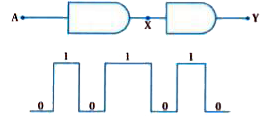
View SolutionA circuit of logic gte made from two AND gate is shown in following figure. Draw output waves for point X. For A and for Y.
View SolutionThe number density of electron is a semiconductor is `8xx10^(13) cm^(-3)` and number density of hole is `5xx10^(12) cm^(-3)` then,
(1) Which type of this semiconductor is?
(2) How much is resistivity of it? (Mobility of electron is 23000 `cm^(2)V^(-1)s^(-1)` and mobility of hole is 100 `cm^(2)V^(-1)s^(-1) and e=1.6xx10^(-19)C`)
View SolutionWhat amount of inpurity of atomic density in added toform N-type semiconductor in Ge semiconductor of conductivity `sigma` is `5Omega^(-1)cm^(-1)` Mobility of electron in N-type semiconductor is 3900 `cm^(2)V^(-1)s^(-1)`. Ignore conductivity due to hole. `(e=1.6xx10^(-19)C)`
View SolutionIf an LED has to emit 662 nm wavelength of light then what should be the band gap energy of its semiconductor? `(h=6.62xx10^(-34)Js)`
View SolutionThe width of a depletion region is 400 nm. The intensity of the electric field at the depletion region is `5xx10^(5)`V/m. Then calculate the following quantities: (1) The value of the potential barrier. (2) The minimum energy required by an electron to move from the n-type to the p-type region of the diode.
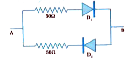
View SolutionFor the circuit shown in the figure, calculate the equivalent resistance for the two cases given as : (1) `V_(A) gt V_(B) and (2) V_(B) gt V_(A)`. Here consider `D_(1) and D_(2)` to be ideal diodes.
View SolutionTherefore are `6xx10^(19)` electrons per unit cubic metre of pure semiconductor. What will be the number of holes for this semiconductor of dimension `1 cm xx 1 cm xx 2 cm`?
View Solution(A) Calculate the value of `V_(0)` and `i` if the silicon and germanium diode start conducting at 0.7 V and 0.3 V respectively.
(B) If the Ge diode connection is now reversed, what will be the new values of `V_(0)` and `i` ?
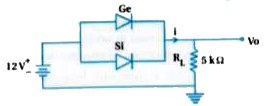
View Solution
Section-B : Numericals (Numerical From .DARPAN. Based On Textbook) questions and complete solutions for chapter SEMICONDUCTOR ELECTRONICS : MATERIALS, DEVICES AND SIMPLE CIRCUITS of KUMAR PRAKASHAN KENDRA PHYSICS (GUJRATI ENGLISH) of Class 12
All Exercises from KUMAR PRAKASHAN Class 12 PHYSICS SEMICONDUCTOR ELECTRONICS : MATERIALS, DEVICES AND SIMPLE CIRCUITS
- Section - A (Try Yourself)
- Section-A : Questions - Answers
- Section-B : Numericals (Numerical From .DARPAN. Based On Textbook)
- Section-B : Numericals (Numerical From Textual Exercise)
- Section-B : Numericals (Numerical From Textual illustrations)
- Section-C: NCERT Exemplar Solution (Long Answer Type Questions)
- Section-C: NCERT Exemplar Solution (Multiple Choice Qustion (MCQs) )
- Section-C: NCERT Exemplar Solution (Multiple Choice Qustion (More than One Options))
- Section-C: NCERT Exemplar Solution (Short Answer Type Questions)
- Section-C: NCERT Exemplar Solution (Very Short Answer Type Questions)
- Section-D : Multiple Choice Questions (MCQs) (MCQs asked in Competitive Exams)
- Section-D : Multiple Choice Questions (MCQs) (MCQs From .DARPAN. Based On Textbook)