Complete Solutions to Section-D : Multiple Choice Questions (MCQs) (MCQs From .DARPAN. Based On Textbook) of chapter SEMICONDUCTOR ELECTRONICS : MATERIALS, DEVICES AND SIMPLE CIRCUITS of Class 12 book with complete answers and questions
| Class 12 | PHYSICS |
| Chapter | SEMICONDUCTOR ELECTRONICS : MATERIALS, DEVICES AND SIMPLE CIRCUITS |
| KUMAR PRAKASHAN | Section-D : Multiple Choice Questions (MCQs) (MCQs From .DARPAN. Based On Textbook) |
| Number Of Questions | 100 |
| Academic Year | 2023-24 |
Which of the following is not a conductor of electricity?
View SolutionAt what temperature semiconductor behaves as conductor?
View SolutionResistivity of semiconductor of approximately ……….. .
View SolutionThe energy band diagram of a Si semiconductor crystal at absolute zero temperature,
View SolutionThe band gaps of a conductor, semiconductor and insulator are respectively `Eg_(1), and Eg_(2) and Eg_(3)`. The relationship between them can be given as ………
View SolutionWhen will the conductivity of a Ge semiconductor decrease?
View SolutionOn increasing the temperature, width forbidden gap ….
View SolutionA piece of copper and piece of germanium and cooled upto 80 K temperature so ……
View SolutionResistivity of metal …… and resistivity on semiconductor …… on temperature decreases
View SolutionGive electronic configuration of silicon.
View SolutionGive electronic configuration of germanium.
View SolutionWhen the semiconductor is heated ……..
View SolutionElectric field is applied to a semiconductor. In it density of conducting charge is n the drift velocity is v. Now increasing the temperature of semiconductor ……..
View SolutionThe density of electron and holes in an intrinsic semiconductor is `n_( e)` and `n_(h)` respectively. Which of the following options are true?
View Solution…… is the charge on hole.
View SolutionHoles and electrons are …..
View SolutionTo prepare the n-type semiconductor from a tetravalent Si or Ge, the impurity atoms of valency …… are chosen.
View SolutionIn intrinsic semiconductor the drift velocity of holes and electron are respectivelty `v_(h) and v_(e )` then, ……..
View SolutionIn a semiconducting material the mobilities of electrons and holes are `mu_(e )` and `mu_(h)` respectively. Which of the following is true?
View SolutionTo make a p-type semiconductor out of pure silicon, it has to mix atoms of …… impurity.
View Solutionp-type semiconductor is formed when ……..
(A) As impurity is mixed in Si.
(B) Al impurity is mixed in Si.
(C ) B impurity is mixed in Ge.
(D) P impurity is mixed in Ge.
View SolutionIs there any benefit to adding trivalent or pentavalent impurity to the copper ?
View SolutionTrivalent and pentavalent impurities are ….., respectively in terms of electric.
View SolutionThe ratio of number density of free electron and hole in p-type semiconductor is …….
View SolutionThe number density of electron is `4.5xx10^(22)m^(-3)` and number density of holes is `4.5xx10^(9)m^(-3)`. This semiconductor is ………..
View SolutionThe number density of electron is `7xx10^(12)m^(-3)` and number density of hole is `7xx10^(12)m^(-3)`. This semiconductor will be ….. Type.
View SolutionWhich of the diagram shown in figure represents variation of total mechanical energy of a pendulum oscillating in air as function of time?
View SolutionWhat is the unit of energy?
View Solutionn-type semiconductor ………
View SolutionIn one atom of As is added per `10^(3)` atoms of Ge then the number of free electron in one mole of Ge will be ……..
View SolutionIf one Al atom added to `10^(9)` per atom of Si then charge on holes in one mole will be ……….
View SolutionIn pure crystal of silicon at 300 K temperature having number of atom `n_(i)=10^(16)m^(-3)`. If `10^(21)` atoms of phosphorus added per `m^(3)` then number of holes created will be …… /`m^(3)`.
View SolutionTherefore are `6xx10^(19)` electrons per unit cubic metre of pure semiconductor. What will be the number of holes for this semiconductor of dimension `1 cm xx 1 cm xx 2 cm`?
View SolutionThe number density of electron is a semiconductor is `8xx10^(13) cm^(-3)` and number density of hole is `5xx10^(12) cm^(-3)` then,
(1) Which type of this semiconductor is?
(2) How much is resistivity of it? (Mobility of electron is 23000 `cm^(2)V^(-1)s^(-1)` and mobility of hole is 100 `cm^(2)V^(-1)s^(-1) and e=1.6xx10^(-19)C`)
View SolutionWhat amount of inpurity of atomic density in added toform N-type semiconductor in Ge semiconductor of conductivity `sigma` is `5Omega^(-1)cm^(-1)` Mobility of electron in N-type semiconductor is 3900 `cm^(2)V^(-1)s^(-1)`. Ignore conductivity due to hole. `(e=1.6xx10^(-19)C)`
View SolutionPotential near the junction in p-n junction is zero then potential at …….. is ………
View SolutionIn p-n junction, depletion barrier near the junction is due to ………
View SolutionIf proportion of impurity is less in p-n junction ……..
View SolutionIf the proportion of impurity increases in semiconductor in p-n junction then depletion region ……….
View SolutionBreakdown voltage means ……..
View SolutionIncreasing forward voltage in diode, the width of depletion layer is ……..
View SolutionThe ratio of resistance of forward bias and reverse bias in p-n connection is …….
View Solutionp-side of semiconductor is earthing and -2V potential applied at n-side so in diode …..
View SolutionWhat is responsible for depletion barrier in depletion layer?
View SolutionWhat is the width n cm of depletion layer in p-n junction?
View SolutionIncreasing reverse bias voltage applied to p-n junction diode ……..
View SolutionKeeping forward bias voltage from 0.6 V to 0.7 V in a p-n junction diode its current become 1 mA to 3mA. The dynamic resistance of diode is …….
View SolutionIn an ammeter 0.2% of main current passes through the galvonometer. If resistance of galvonometer is G, the resistance of ammeter will be _____
View SolutionIn an ammeter 0.2% of main current passes through the galvonometer. If resistance of galvonometer is G, the resistance of ammeter will be _____
View SolutionWhen p-n junction diode is forward biased ………
View SolutionA spring of force constant k is kept in the compressesd condition between two blocks masses m and M on the smooth surface of a table as shown in figure .When the spring is released , both the blocks move in opposite directions .When the spring attains the orginal (normal ) position . both blocks lose the constacts with the spring . If x is the intial compression of the spring find the speeds of block while getting detached from the spring .

View Solution
In the circuit shown in figure, if the diode forward voltage drop is 0.3 V, the voltage difference between A and B is
View SolutionIn a zener diode, the reverse bias voltage is 3V and width of the depletion region is 300 Å, the electric field intensity will be ……., `(V)/(cm)`.
View SolutionWhat is order of current flowing during lightening in the sky ?
View SolutionThe current is flowing through solenoid, then solenoid acting as what ?
View SolutionThe potential barrier of 0.5 V exist across a p-n junction. If the dpletion region is `5.0xx10^(-7)m` wide, then the intensity of electric field in this region is ………….
View SolutionWhich of the following is true ?
View SolutionWhich of the following does not result in an increase in the entropy?
View Solution3 identical capacitors are joined in parallel and are charged with a battery of 10 V. Now the battery is removed and they are joined in series with each other in this condition what would be the potential difference between the freed plates in the combination?
View SolutionWhen p.d between two ends of secondary of full wave rectification is 100 V then in p-n junction p.d. is …… between p and n in reverse bias.
View SolutionWe get ….. Current through rectifier without simple filter.
View SolutionAn A.C. supply of 350 V, 60 Hz is applied to a full wave rectifier. If internal resistance of each diode is `200Omega` and load resistance `R_(1)=5k Omega`, then the maximum value of output current is …….
View SolutionConsider a current carrying wire (current I) in the shape of a circle. Note that as the current progresses along the wire, the direction of J (current density) changes in an exact manner, while the current I remain unaffected. The agent that is essentially responsible for is
View SolutionWhich of the following is true ?
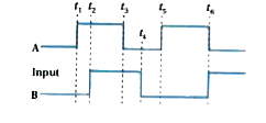
View SolutionJustify the output waveform (Y) of the OR gate for the following inputs A and B given in figure.
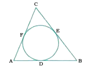
View SolutionIn the given figure, if `AB = 12cm. BC = 8cm` and `AC = 10 cm,` then` AD = ………cm`
View SolutionTo easily obtain the zener effect ……..
View SolutionThe network shown in figure is a part of the circuit. (The battery has negligible resistance)

At a certain instant the current I = 5A and is decreasing at a rate of `10^3 As^(-1)`. What is the potential difference between point B and A ?
View Solution
In the circuit shown in figure, if the diode forward voltage drop is 0.3 V, the voltage difference between A and B is
View SolutionThe breakdown voltage of a zener diode is `V_(Z)`. It is connected to the supply of V volts, so which of the following options for diode will act as regulated voltage?
View SolutionWhich diode converts light waves into electrical signals in the absence of external battery?
View SolutionThe band gap of the semiconductor of the LED that produces the visual light is at least ……
View Solution…… do not always have to be Sunshine.
View SolutionFinger shape anode is used in ………
View SolutionAt breakdown voltage the reverse current of p-n junction can be ranked mA ……. .
View SolutionIf the incident wavelength on a photodiode is 1700 nm, what is its energy gap `(E_(g))` ?
View SolutionGiving 2V to LED passes a 10 mA current. If you want to connect this diode to a 6V battery, then the value of resistance in series kept……
View SolutionIf the maximum load voltage of 40 V is to be obtained from the bridge rectifier, the value of rms from the secondary is approximately ………
View SolutionWhen we use zener diode as a voltage regulator, its connection …….
(i) forward bias
(ii) reverse bias
(iii) should parallel with load
(iv) should series with load
View SolutionThe heat produced per unit time, on passing electric current through a conductor at a given temperature is directly proportional to the .....
View SolutionTo get light in visible region through LED …….. Semiconductor is used.
View SolutionForward bias has to be provided for the ….. Semiconductor device to work.
View Solution
In the circuit shown in figure, if the diode forward voltage drop is 0.3 V, the voltage difference between A and B is
View SolutionWhat is the difference between cutaneous and pulmonary respiration ?
View SolutionThe circuit symbol of LED, p-n junction diode is …..
View SolutionWhich of the following is true ?
View SolutionWhich of the following in true for Golden rice ?
View Solution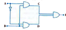
Truth table for the given circuit (See figure) is
View SolutionWhich of the following in true for Golden rice ?
View SolutionWhich gate does not require a p-n junction diode?
View SolutionNAND gate is combination of ….. gate and …….. gate.
View SolutionNOR gate is the combination of ….. Gate and …… gate.
View Solution….. NAND gate is required for OR gate.
View Solution……NOT gate is required for NAND gate.
View SolutionWhich of the following logic gate is an universal gate?
View SolutionWhich of the following logic gate is an universal gate?
View SolutionWhich of the following is true ?
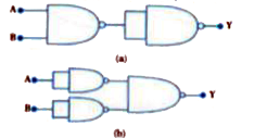
View SolutionYou are given the circuits as shown in figure, which consist of NAND gates. Identify the logic operation carried out by the two circuits.
View SolutionJustify the output waveform (Y) of the OR gate for the following inputs A and B given in figure.

View SolutionWrite the truth table for a NAND gate connected as given in figure.

Hence identify the exact logic operation carried out by this circuit.
View Solution
Section-D : Multiple Choice Questions (MCQs) (MCQs From .DARPAN. Based On Textbook) questions and complete solutions for chapter SEMICONDUCTOR ELECTRONICS : MATERIALS, DEVICES AND SIMPLE CIRCUITS of KUMAR PRAKASHAN KENDRA PHYSICS (GUJRATI ENGLISH) of Class 12
All Exercises from KUMAR PRAKASHAN Class 12 PHYSICS SEMICONDUCTOR ELECTRONICS : MATERIALS, DEVICES AND SIMPLE CIRCUITS
- Section - A (Try Yourself)
- Section-A : Questions - Answers
- Section-B : Numericals (Numerical From .DARPAN. Based On Textbook)
- Section-B : Numericals (Numerical From Textual Exercise)
- Section-B : Numericals (Numerical From Textual illustrations)
- Section-C: NCERT Exemplar Solution (Long Answer Type Questions)
- Section-C: NCERT Exemplar Solution (Multiple Choice Qustion (MCQs) )
- Section-C: NCERT Exemplar Solution (Multiple Choice Qustion (More than One Options))
- Section-C: NCERT Exemplar Solution (Short Answer Type Questions)
- Section-C: NCERT Exemplar Solution (Very Short Answer Type Questions)
- Section-D : Multiple Choice Questions (MCQs) (MCQs asked in Competitive Exams)
- Section-D : Multiple Choice Questions (MCQs) (MCQs From .DARPAN. Based On Textbook)