Complete Solutions to Section-D : Multiple Choice Questions (MCQs) (MCQs asked in Competitive Exams) of chapter SEMICONDUCTOR ELECTRONICS : MATERIALS, DEVICES AND SIMPLE CIRCUITS of Class 12 book with complete answers and questions
| Class 12 | PHYSICS |
| Chapter | SEMICONDUCTOR ELECTRONICS : MATERIALS, DEVICES AND SIMPLE CIRCUITS |
| KUMAR PRAKASHAN | Section-D : Multiple Choice Questions (MCQs) (MCQs asked in Competitive Exams) |
| Number Of Questions | 100 |
| Academic Year | 2023-24 |
At absolute zero temperature Si acts as ……..
View SolutionThe energy band gap is maximum in …….
View SolutionFormation of covalent bonds in compounds exhibits …….nature.
View SolutionBy increasing the temperature, the specific resistance of a conductor and a semiconductor.
View SolutionThe difference in the variation of resistance with temperature in a metal and a semiconductor arises essentially due to the difference in the ……….
View SolutionIn the middle of the electron layer of a reverse biased p-n junction, the ……
View SolutionA piece of copper and another of germanium are cooled from room temperature to 77 K, the resistance of ……….
View SolutionThe manifestion of band structure in solids is due to …….
View SolutionWhen p-n junction diode is forward biased ………
View SolutionThe electrical conductivity of a semiconductor of a semiconductor increases when electromagnetic radiation of wavelength shorter than 2480 nm, is incident on it. The band gap in (eV) for the semi conductor is ……
View SolutionIn a full wave rectifier circuit operating from 50 Hz mains frequency, the fundamental frequency in the ripple would be ………
View SolutionRatio of number density of holes is `(7)/(5)` and ratio of their current is `(7)/(4)` in a semiconductor. The ratio of their drift velocity is …….
View SolutionWhich of the following is true ?
View SolutionA charge of `2 xx 10^(-2) ` C moves at 30 revolutions per second in a circle of diameter 80 cm. The current linked with the circuit is .....
View SolutionA solid which is transparent to visible light an whose conductivity increases with temperature is formed by ……..
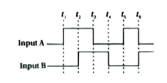
View SolutionAs shown in the following figure take A and B input waveforms. Sketch the output waveform obtained from NAND gate.
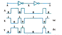
View SolutionA logic circuit is shown in the diagram. Draw the output signal at the point X and Y for the input signal shown in the figure at point A.
View SolutionCarbon, silicon and germanium have four valence electrons each. At room temperature which one of the following statements is most appropriate?
View SolutionFigure shows electric field lines in which an electric dipole P is placed as shown. Which of the following statements is correct ?

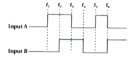
View SolutionAs shown in the following figure, take A and B input waveforms. Sketch the output waveform obtained from AND gate.
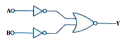
View SolutionWhich logic gate is represented by the following logic gates?
View SolutionIf the output of the OR gate is connected to both inputs of the NAND gate, then this combination acts as a ……….
View SolutionWrite the truth table for a NAND gate connected as given in figure.

Hence identify the exact logic operation carried out by this circuit.
View SolutionWhy is `I to V` characteristic of a solar cell draw in the fourth quadrant of the coordinate system?
View SolutionWhich of the following is correct
View SolutionIf A and B are invertible matrices, then which of the following is not correct
View SolutionBelow is a list of plant fibres. From which part of the plant these are obtained ?
(a) Coir (b) Hemp (c) Cotton (d) jute
View SolutionFor common emitter configuration, if `alpha and beta` have their usual meanings, the incorrect relationship between `alpha and beta` is :
View SolutionIf X is the number of tails in three tosses of a coin, determine the standard deviation of X.
View SolutionIn a common emitter amplifier circuit using a n-p-n transistor, the phase difference between the input and the output voltages will be ……..
View Solution
The output of the given circuit in figure.
View Solution
In the circuit shown in figure, if the diode forward voltage drop is 0.3 V, the voltage difference between A and B is
View SolutionWhich of the following is true ?
View SolutionWhat is the difference between a nucleotide and nucleoside ? Give two examples of each with their structure.
View SolutionDerive an expression for current I passing through an AC circuit containing only inductor L. Draw a Phasor diagram and graph of v and I versus `omega t`. Explain instantaneous power and the average power.
View SolutionThe depletion layer in the p-n junction region is caused by ……
View SolutionWhen a p-n junction diode is reverse biased, the flow of current across the junction is maninly due to ……..
View SolutionThe output of OR gate is 1 ……..
View SolutionBarrier potential of a p-n junction diode does note depend on …….
View SolutionWhich gate will be obtained by joining the two inputs of the NAND gate?
View SolutionReverse bias applied to a junction diode ……
View SolutionIn semiconductor at a room temperature ………
View SolutionThe peak voltage in the output of a half wave diode rectifier fed with a sinusoidal signal without filter is 10V. The d.c. component of the output voltage is ……..
View SolutionThe output of OR gate is 1 ……..
View SolutionChoose the only false statement from the following.
View SolutionApplication of a forward bias to a p-n junction ………
View SolutionZener diode use for ….
View SolutionAn AND gate is followed by a NOT gate in series with two inputs A and B, the Boolean expresion for the output Y will be ……….
View SolutionJustify the output waveform (Y) of the OR gate for the following inputs A and B given in figure.
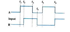
View SolutionIn a semiconducting material the mobilities of electrons and holes are `mu_(e )` and `mu_(h)` respectively. Which of the following is true?
View SolutionA p-n photodiode is made of a material with a band gap of 2.0 eV. The minimum frequency of the radiation that can be absorbed by the material is nearly ……
View SolutionObtain the resonant frequency and Q-factor of a series LCR circuit with `L = 3.0 H, C = 27 muF, and R = 7.4 Omega`. It is desired to improve the sharpness of the resonance of the circuit by reducing its ‘full width at half maximum’ by a factor of 2. Suggest a suitable way.
View SolutionA gas in equilibrium has uniform density and pressure throughout its volume. This is strictly true only if there are no external influences. A gas column under gravity, for example, does not have uniform density (and pressure). As you might expect, its density decreases with height. The precise dependence is given by the so-called law of atmospheres
`n_(2)= n_(1) "exp"[-mg(h_(2)-h_(1))//k_(B)T]`
where `n_(2), n_(1)` refer to number density at heights `h_(2)` and `h_(1)` respectively. Use this relation to derive the equation for sedimentation equilibrium of a suspension in a liquid column:
`n_(2)= n_(1)"exp"[ -mgN_(A)(rho-rho')(h_(2)-h_(1))//rhoRT)]` where `rho` is the density of the suspended particle, and `rho'`, that of surrounding medium. [`N_(A)` is Avogadro's number, and R the universal gas constant.] [Hint : Use Archimedes principle to find the apparent weight of the suspended particle.]
View SolutionA p-n photodiode is fabricated from a semiconductor with a band gap of 2.5 eV. It can detect a signal of wavelength ……..
View SolutionWhich one of the following statement is false?
View SolutionWhich of the following device acts a complete electronic circuit?
View SolutionWhich of the following statement is true for the forward bias of a p-n junction?
View SolutionIf a small amount of antimony is added to germanium crystal ………
View SolutionPure Si at 500 K has equal number of electron `(n_(e ))` and hole `(n_(h))` concentrations of `1.5xx10^(16)m^(-3)`. Doping by indium increases `n_(h)` to `4.5xx10^(22)m^(-3)`. The doped semiconductor is of ………
View SolutionKeeping forward bias voltage from 0.6 V to 0.7 V in a p-n junction diode its current become 1 mA to 3mA. The dynamic resistance of diode is …….
View SolutionIn a CE transistor amplifier, the audio signal voltage across the collector resistance of `2kOmega` is 2V. If the base resistance is `1kOmega` and the current amplification of the transistor is 100, the input signal voltage is ………..
View SolutionC and Si both have same lattice structure, having 4 bonding electrons in each. However, C is insulator where as Si is intrinsic semiconductor. This is because, …….
View SolutionWhen the inputs of a two input logic gate are 0 and 0, the output is 1, when the inputs are 1 and 0, the output is zero. The type of logic gate …..
View SolutionJustify the output waveform (Y) of the OR gate for the following inputs A and B given in figure.

View Solution
The output of the given circuit in figure.
View SolutionIn a n-type semiconductor, which of the following statement is true?
View SolutionThe potential barrier of the p-n junction depends ……..
(i) On kind of semiconductor material (ii) On amount of doping (iii) On temperature
View SolutionIn a n-type semiconductor, which of the following statement is true?
View SolutionA helicopter is moving in upward direction with speed of 10 m/s. If the length of the helicopter is 10 m and the horizontal component of magnetic field of earth is `1.5 xx 10^(-3) "Wb"/ m^2` then the induced emf produced across the foremost (nose) and end part (tail) of the helicopter will be ____
View SolutionWhich logic gate is represented by the following logic gates?

View SolutionA cell of emf E and internal resistance r is connected across an external resistance R. Plot a graph showing the variation of P.D. across R, verses R.
View SolutionDerive an expression for current I passing through an AC circuit containing only inductor L. Draw a Phasor diagram and graph of v and I versus `omega t`. Explain instantaneous power and the average power.
View SolutionIn the circuit shown the reading of voltmeter `V_(3)` and Ammeter 'A' will be
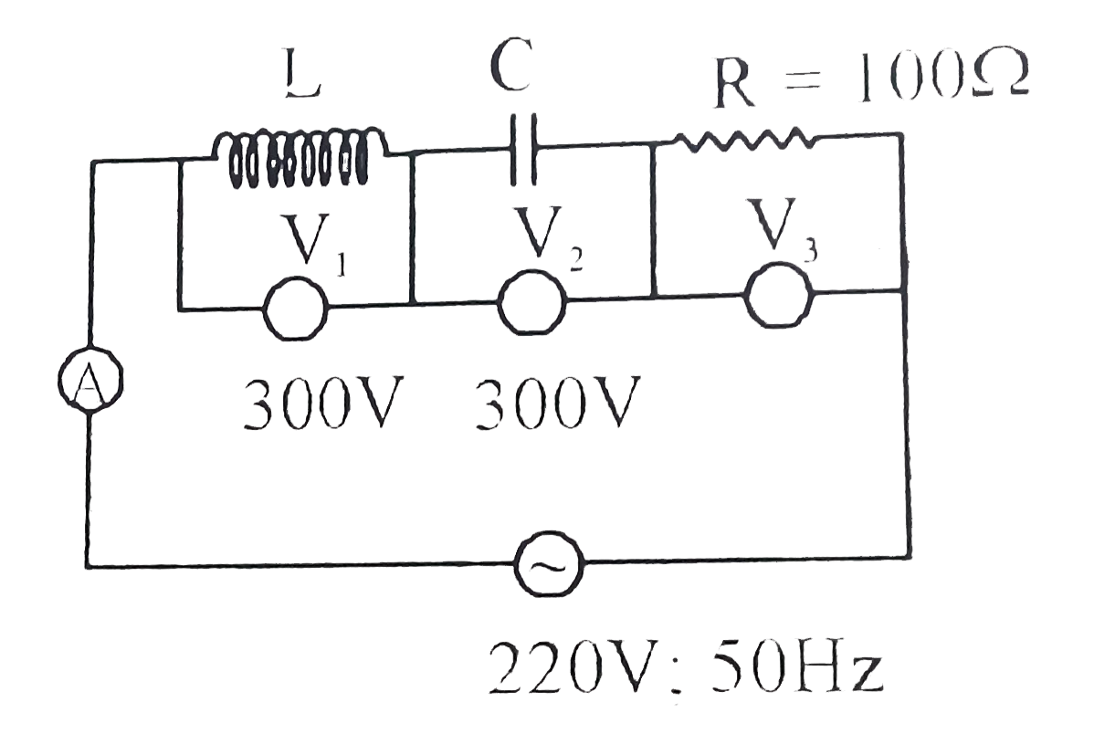
View SolutionJustify the output waveform (Y) of the OR gate for the following inputs A and B given in figure.

View SolutionIf A and B are two matrices of the order `3xxmand3xxn` , respectively , and m=n , then the order of matrix `(5A-2B)` is ……….
View SolutionWhich of the following logic gate is an universal gate?
View Solution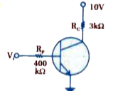
In the circuit shown in figure, when the input voltage of the base resistance is 10V, `V_(BE)` is zero and `V_(CE)` is also zero. Find the values of `I_(B), I_(C ) and beta`.
View SolutionIn a p-n junction diode, change in the temperature due to heating …….
View SolutionWhich of the following can be used as a biocontrol agent in the treatment of plant disease ?
View SolutionFor a p-type semiconductor, which of the following statements is true?
View SolutionObtain the resonant frequency and Q-factor of a series LCR circuit with `L = 3.0 H, C = 27 muF, and R = 7.4 Omega`. It is desired to improve the sharpness of the resonance of the circuit by reducing its ‘full width at half maximum’ by a factor of 2. Suggest a suitable way.
View SolutionA circular loop enters a uniform magnetic field as shown in the figure. The current induced in the coil ____
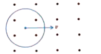
View SolutionThe rms value of a.c. signal in halfwave rectifier is ……
View SolutionThe valency of the impurity atom added to make germanium crystal into n-type semi-conductor have ….
View SolutionTo a germanium sample, traces of galium are added as an impurity. The resultant sample would behave like ……..
View SolutionWhen the semiconductor is heated ……..
View SolutionWhich logic gate is represented by the following logic gates?

View SolutionA Ge specimen is doped with Al. The concentration of acceptor atoms is `10^(21)"atoms/m"^(3)`. Given that the intrinsic concentration of electron hole pairs is `10^(19)//m^(3)`, the concentration of electrons in the specimen is …….
View SolutionWhich of the following logic gate is an universal gate?
View SolutionWrite the truth table for circuit given in figure below consisting of NOR gates and identify the logic operation (OR, AND, NOT) which this circuit is performing.

View SolutionA light emitting diode (LED) has a voltage drop of 2 volt across it and passes a current of 10 mA when it operates with a 6 volt battery through a limiting register R. The value of R is ……
View SolutionIn half wave rectification, what is the output frequency if the input frequency is 50 Hz.
View SolutionThe forbidden gap in the energy bonds of silicons is ……
View SolutionWhich among the following is applicable to tapetum?
(A) Protective layer
(B) Nourishing layer
(C) Vestigial part
(D) None of the above
View SolutionWhen the inputs of a two input logic gate are 0 and 0, the output is 1, when the inputs are 1 and 0, the output is zero. The type of logic gate …..
View SolutionWhich logic gate is represented by the following logic gates?

View SolutionThe direction of the electric field in p-n junction diode is …….
View SolutionWhen the electromagnetic radiation of maximum wavelength of 2480 nm is incident on semiconductor. The band gap energy of semiconductor is ……eV. `[6.6xx10^(-34)JS, C=3xx10^(8)m//s, 1eV=1.6xx10^(-19)J]`
View SolutionTo create AND gate require ……NAND gate.
View SolutionWhat kind of p-n junction diode does not require any kind of bias?
View Solution
Section-D : Multiple Choice Questions (MCQs) (MCQs asked in Competitive Exams) questions and complete solutions for chapter SEMICONDUCTOR ELECTRONICS : MATERIALS, DEVICES AND SIMPLE CIRCUITS of KUMAR PRAKASHAN KENDRA PHYSICS (GUJRATI ENGLISH) of Class 12
All Exercises from KUMAR PRAKASHAN Class 12 PHYSICS SEMICONDUCTOR ELECTRONICS : MATERIALS, DEVICES AND SIMPLE CIRCUITS
- Section - A (Try Yourself)
- Section-A : Questions - Answers
- Section-B : Numericals (Numerical From .DARPAN. Based On Textbook)
- Section-B : Numericals (Numerical From Textual Exercise)
- Section-B : Numericals (Numerical From Textual illustrations)
- Section-C: NCERT Exemplar Solution (Long Answer Type Questions)
- Section-C: NCERT Exemplar Solution (Multiple Choice Qustion (MCQs) )
- Section-C: NCERT Exemplar Solution (Multiple Choice Qustion (More than One Options))
- Section-C: NCERT Exemplar Solution (Short Answer Type Questions)
- Section-C: NCERT Exemplar Solution (Very Short Answer Type Questions)
- Section-D : Multiple Choice Questions (MCQs) (MCQs asked in Competitive Exams)
- Section-D : Multiple Choice Questions (MCQs) (MCQs From .DARPAN. Based On Textbook)