Complete Solutions to Section-C: NCERT Exemplar Solution (Long Answer Type Questions) of chapter SEMICONDUCTOR ELECTRONICS : MATERIALS, DEVICES AND SIMPLE CIRCUITS of Class 12 book with complete answers and questions
| Class 12 | PHYSICS |
| Chapter | SEMICONDUCTOR ELECTRONICS : MATERIALS, DEVICES AND SIMPLE CIRCUITS |
| KUMAR PRAKASHAN | Section-C: NCERT Exemplar Solution (Long Answer Type Questions) |
| Number Of Questions | 10 |
| Academic Year | 2023-24 |
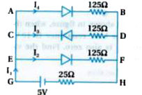
If each diode in figure has a forward bias resistance of `25Omega` and infinite resistance in reverse bias, what will be the values of the current `I_(1), I_(2), I_(3) and I_(4)`?
View Solution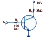
In the circuit shown in figure, when the input voltage of the base resistance is 10V, `V_(BE)` is zero and `V_(CE)` is also zero. Find the values of `I_(B), I_(C ) and beta`.
View Solution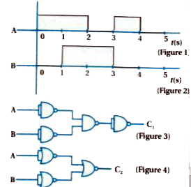
Draw the output signals `C_(1) and C_(2)` in the given combination of gates as shown in figure.
View Solution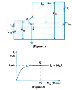
Consider the circuit arrangement shown in figure (1) for studying input and output characteristics of n-p-n transistor in CE configuration.
Select the values of `R_(B)` and `R_(C )` for a transistor whose `V_(BE)=0.7V`, so that the transistor is operating at point Q as shown in the characteristics shown in figure (2). Given that the input impedance of the transistor is very small and `V_(C C)=V_(BB)=16V`, also find the voltage gain and power gain of circuit making appropriate assumptions.
View Solution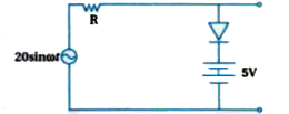
Assuming the ideal diode, draw the output waveform for the circuit given in figure. Explain the waveform.
View SolutionSuppose a 'n'-type wafer is created by dopin Si crystal having `5xx10^(28)` atoms/`m^(3)` with 1 ppm concentration of As. On the surface 200 ppm Boron is added to create 'P' region in this wafer. Considering `n_(i)=1.5xx10^(16)m^(-3)` (i) Calculate the denisties of the charge carrier in the n & p regions. (ii) Comment which charge carriers would contribute largely for the reverse saturation current when diode is reverse biased.
View SolutionAn X-OR gate has following truth table:

It is represented by following logic relation
`Y=barA.B+A.barB`
Build this gate using AND, OR and NOT gates.
View SolutionConsider a box with three terminals on top of it as shown in figure (a)
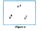
Three components namely, two germanium diodes and one resistor are connected across these three terminals in some arrangement. A student performs an experiment in which any two of these three terminals are connected in the circuit shown in figure (b).

The student obtains graphs of current-voltage characteristics for unknown combination of components between the two terminals connected in the ciruit.
The graphs are :
(i) When A is positive and B is negative

(ii) When A is negative and B is positive

(iii) When B is negative and C is positive

(iv) When B is positive and C is negative

(v) When A is positive and C is negative

(vi) When A is negative and C is positive

From these graphs of current - voltage characteristic shown in figure (c ) to (h), determine the arrangement of components between A, B and C.
View Solution
In the circuit shown in figure, when the input voltage of the base resistance is 10V, `V_(BE)` is zero and `V_(CE)` is also zero. Find the values of `I_(B), I_(C ) and beta`.
View Solution
The output of the given circuit in figure.
View Solution
Section-C: NCERT Exemplar Solution (Long Answer Type Questions) questions and complete solutions for chapter SEMICONDUCTOR ELECTRONICS : MATERIALS, DEVICES AND SIMPLE CIRCUITS of KUMAR PRAKASHAN KENDRA PHYSICS (GUJRATI ENGLISH) of Class 12
All Exercises from KUMAR PRAKASHAN Class 12 PHYSICS SEMICONDUCTOR ELECTRONICS : MATERIALS, DEVICES AND SIMPLE CIRCUITS
- Section - A (Try Yourself)
- Section-A : Questions - Answers
- Section-B : Numericals (Numerical From .DARPAN. Based On Textbook)
- Section-B : Numericals (Numerical From Textual Exercise)
- Section-B : Numericals (Numerical From Textual illustrations)
- Section-C: NCERT Exemplar Solution (Long Answer Type Questions)
- Section-C: NCERT Exemplar Solution (Multiple Choice Qustion (MCQs) )
- Section-C: NCERT Exemplar Solution (Multiple Choice Qustion (More than One Options))
- Section-C: NCERT Exemplar Solution (Short Answer Type Questions)
- Section-C: NCERT Exemplar Solution (Very Short Answer Type Questions)
- Section-D : Multiple Choice Questions (MCQs) (MCQs asked in Competitive Exams)
- Section-D : Multiple Choice Questions (MCQs) (MCQs From .DARPAN. Based On Textbook)