Complete Solutions to Section-B : Numericals (Numerical From Textual illustrations) of chapter SEMICONDUCTOR ELECTRONICS : MATERIALS, DEVICES AND SIMPLE CIRCUITS of Class 12 book with complete answers and questions
| Class 12 | PHYSICS |
| Chapter | SEMICONDUCTOR ELECTRONICS : MATERIALS, DEVICES AND SIMPLE CIRCUITS |
| KUMAR PRAKASHAN | Section-B : Numericals (Numerical From Textual illustrations) |
| Number Of Questions | 16 |
| Academic Year | 2023-24 |
C, Si and Ge have same lattice structure. Why is C insulator while Si and Ge intrinsic semiconductors?
View SolutionSn, Si and Ge have the same lattice structure . Why Sn is a conductor while Si and Ge are Semiconductor?
View SolutionSuppose a pure Si crystal has `5xx10^(28)` atoms `m^(-3)`. It is doped by 1 ppm concentration of pentavalent As. Calculate the number of electrons and holes. Given that `n_(i)=1.5xx10^(16)m^(-3)`.
View SolutionAt temperature 300 K number density of electrons and holes in pure silicon is `1.5xx10^(16)m^(-3)`. The number density of hole increase by `4.5xx10^(22)m^(-3)` dopping the indium impurity so calculate number denstiy of electron.
View SolutionCan we take one slab of p-type semiconductor and physically join it to another n-type semiconductor to get p-n junction?
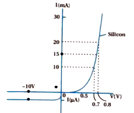
View SolutionThe `V to I` characteristic of a silicon diode is shown in the figure. Calculate the resistance of the diode at (a) `I_(D)=15mA` and (b) `V_(D)=-10V`.
View SolutionThe values of voltage V and current I for a given diode are given in the following table.

Find the forward bias resistance and reverse bias resistance for a given diode for a straight line characteristics.
View SolutionIn a Zener regulated power supply a Zener diode with `V_(Z)=6.0V` is used for regulation. The load current is to be 4.0 mA and the unregulated input is 10.0V. What should be the value of series resistor `R_(S)`?
View SolutionThe current in the forward bias is known to be more `(~mA)` than the current in the reverse bias `(~muA)`. What is the reason then to operate the photodiodes in reverse bias?
View SolutionWhy are Si and GaAs are perferred materials for solar cells?
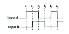
View SolutionJustify the output waveform (Y) of the OR gate for the following inputs A and B given in figure.
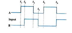
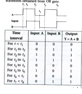
View SolutionThe digital signal for the OR gate with two inputs is shown in the figure. Sketch the output waveform obtained from OR gate.
View SolutionAs shown in the following figure, take A and B input waveforms. Sketch the output waveform obtained from AND gate.
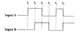
View SolutionAs shown in the following figure, take A and B input waveforms. Sketch the output waveform obtained from AND gate.

View SolutionJustify the output waveform (Y) of the OR gate for the following inputs A and B given in figure.

View SolutionAs shown in the following figure take A and B input waveforms. Sketch the output waveform obtained from NAND gate.
View Solution
Section-B : Numericals (Numerical From Textual illustrations) questions and complete solutions for chapter SEMICONDUCTOR ELECTRONICS : MATERIALS, DEVICES AND SIMPLE CIRCUITS of KUMAR PRAKASHAN KENDRA PHYSICS (GUJRATI ENGLISH) of Class 12
All Exercises from KUMAR PRAKASHAN Class 12 PHYSICS SEMICONDUCTOR ELECTRONICS : MATERIALS, DEVICES AND SIMPLE CIRCUITS
- Section - A (Try Yourself)
- Section-A : Questions - Answers
- Section-B : Numericals (Numerical From .DARPAN. Based On Textbook)
- Section-B : Numericals (Numerical From Textual Exercise)
- Section-B : Numericals (Numerical From Textual illustrations)
- Section-C: NCERT Exemplar Solution (Long Answer Type Questions)
- Section-C: NCERT Exemplar Solution (Multiple Choice Qustion (MCQs) )
- Section-C: NCERT Exemplar Solution (Multiple Choice Qustion (More than One Options))
- Section-C: NCERT Exemplar Solution (Short Answer Type Questions)
- Section-C: NCERT Exemplar Solution (Very Short Answer Type Questions)
- Section-D : Multiple Choice Questions (MCQs) (MCQs asked in Competitive Exams)
- Section-D : Multiple Choice Questions (MCQs) (MCQs From .DARPAN. Based On Textbook)