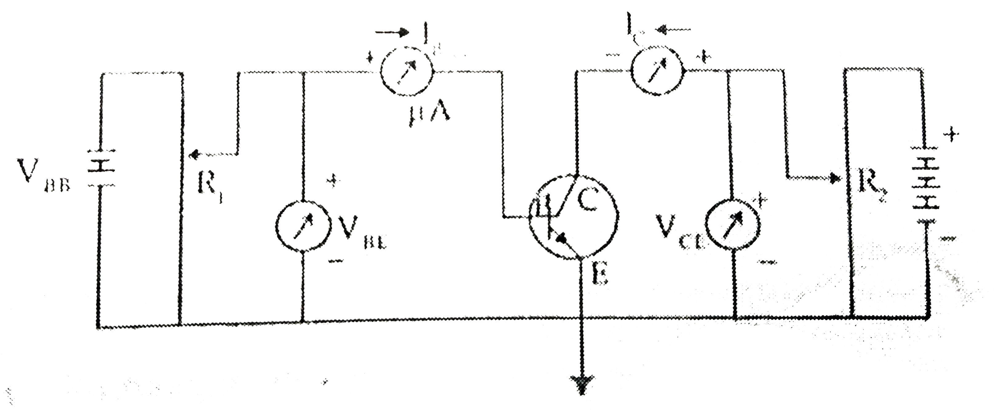
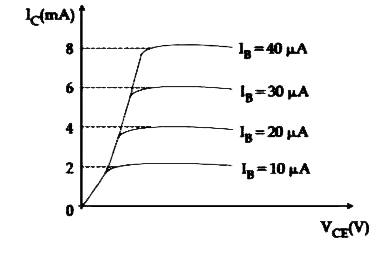
(i) Draw a circuit diagram to study the input and output characteristics of an n-p transistor in its common emitter configuration. Draw the typical input and output characteristics.
(ii) Explain, with the hepl of a circuit diagram, the working of n-p transistor as a common emitter amplifier.
(i) The circuit arrangement to obtain the characteristics of a n-p transistor is shown in figure.
Input characteristic : Input characteristics are graph between VBEandIB at constant VCE
Output characteristics : Output characteristics are graph between VCEandIC at constant IB

(ii) Transistor amplifier is based on the principle that a weak input signal given to base region produces an amplified (large) output signal in the collector region.

A simple amplifier circuit in common emitted configuration using a n-p-n transistor has been shown in Fig. The input signal vi is connected between base and emitter through a capacitor C1, which blocks d.c. voltage VBB from going towards the a.c. input source. The output is taken from the collector resistance RC. The capacitor C2 blocks the d.c. voltage VCC from the output signal v0
Due to input signal the base current changes by a value iB=viRB and correspondingly collector current changes by
iC=βiB=βviRB
∴ Output voltage across RC will be
v0=RC.iC=βRCRBvior Voltage gain Av=v0vi=β.RCRB
The input and output wavefronts have been shown in fig.(b) and (c), respectively. The output is amplified but is in opposite phase i.e., the input differ in phase by 180∘orπ radian.
Topper's Solved these Questions
- XII BOARDSBOOK - XII BOARDS PREVIOUS YEARCHAPTER - XII BOARDSEXERCISE - SET II
9 Videos
- XII BOARDSBOOK - XII BOARDS PREVIOUS YEARCHAPTER - XII BOARDSEXERCISE - SET III
9 Videos
- XII BOARDSBOOK - XII BOARDS PREVIOUS YEARCHAPTER - XII BOARDSEXERCISE - SECTION - B
9 Videos
- SAMPLE PAPER 2019BOOK - XII BOARDS PREVIOUS YEARCHAPTER - SAMPLE PAPER 2019EXERCISE - SECTION D
6 Videos
Similar Questions
(i) Draw a circuit diagram to study the input and output characteristics of an n-p-n transistor in its common emitter configuration. Draw the typical input and output characteristics.
(ii) Explain, with the hepl of a circuit diagram, the working of n-p-n transistor as a common emitter amplifier.
View SolutionDraw a circuit diagram to obtain the characteristics of a n-p-n transistor in common base configuration . Give shape of input and output characteristic curves.
View SolutionDefine the dynamic output resistance of a transistor amplifier in common - emitter configuration.
View SolutionDraw a circuit diagram to study characteristics of a transistor (pnp or ppn) in common emitter configuration. Draw the sketch of (i) input characterisitics and (ii) output characteristics for this configuration.
View SolutionDraw circuit diagram for n-p-n transistor to draw input and output characteristics in common base configuration. Draw the input and ouput curves and explain them.
View SolutionExplain the input and output characteristics curves for a common emitter transistor.
View SolutionDraw a circuit diagram to study characteristics of n-p-n transistor in CE configuration. Draw the sketch of input and output characteristics of this configuration . Define current amplification factor ?
View SolutionThe typical output characteristics curve for a transistor working in the common-emitter configuration is shown in the figure.

View SolutionWith the help of a labelled circuit diagram, explain how an n-p-n transistor can be used as an amplifier in common-emitter configuration. Explain how the input and output voltages are out of phase by 180 for a common-emitter transistor amplifier.
View SolutionDraw the circuit diagram for studying the characteristics of a transistor in common emitter configuration. Explain briefly and show how input and output characteristics are drawn.
View Solution
