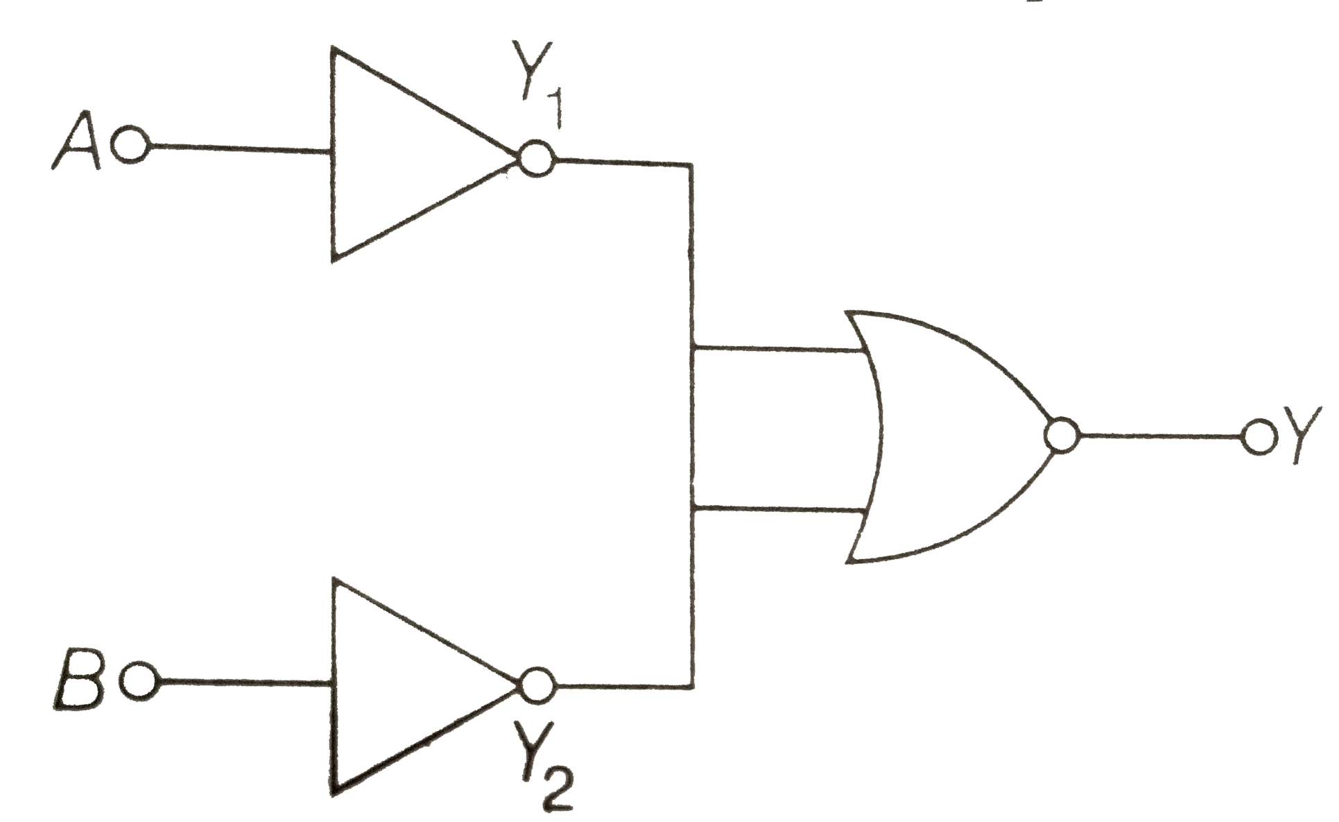
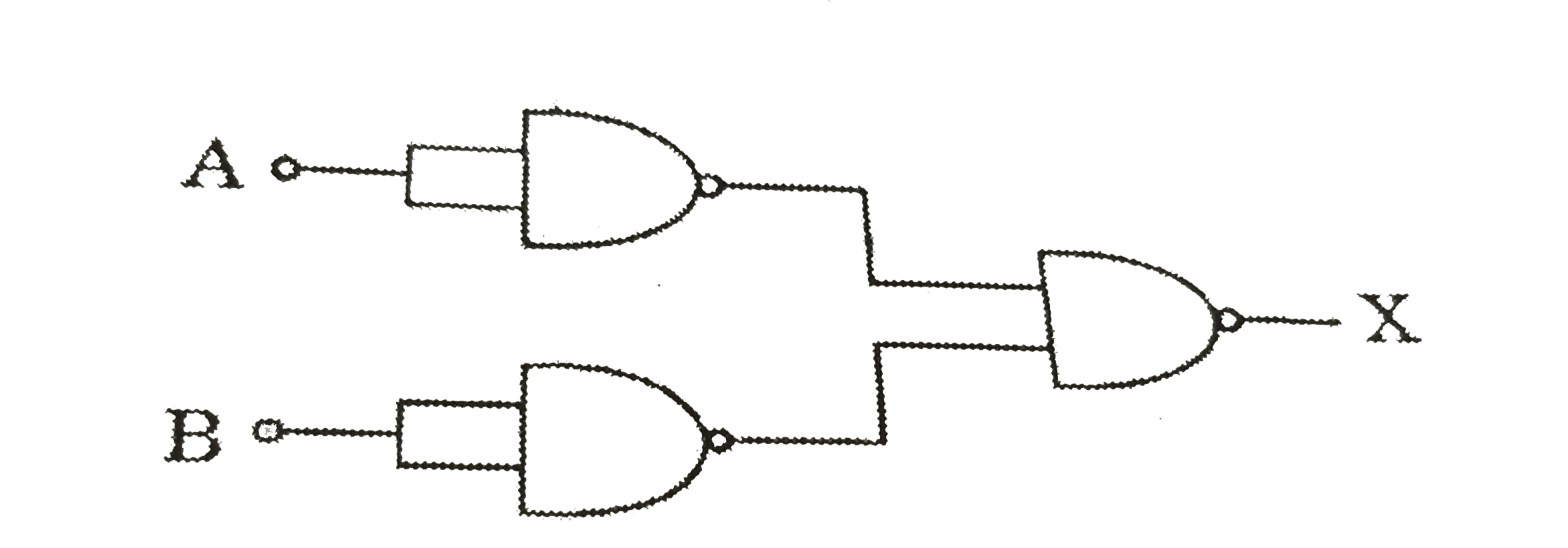
Which logic gate is represented by the following combination of logic gates?
OR
NAND
AND
NOR
The correct Answer is:C
Y=¯¯¯¯¯¯¯¯¯¯¯¯¯¯¯A+¯¯¯B=¯¯¯¯¯¯¯A.¯¯¯¯¯¯B=A.B=AND gate
Topper's Solved these Questions
- BOOK - ALLENCHAPTER - SEMICONDUCTORSEXERCISE - Part-3(Exercise-2)49videos
SEMICONDUCTORS
- BOOK - ALLENCHAPTER - SEMICONDUCTORSEXERCISE - Part-3(Exercise-3)27videos
SEMICONDUCTORS
- BOOK - ALLENCHAPTER - SEMICONDUCTORSEXERCISE - Part-3(Exercise-4)51videos
SEMICONDUCTORS
- BOOK - ALLENCHAPTER - PHYSICAL WORLD, UNITS AND DIMENSIONS & ERRORS IN MEASUREMENT EXERCISE - EXERCISE-IV8videos
PHYSICAL WORLD, UNITS AND DIMENSIONS & ERRORS IN MEASUREMENT
- BOOK - ALLENCHAPTER - WAVES AND OSCILLATIONSEXERCISE - Part-1(Exercise-05)[B]42videos
WAVES AND OSCILLATIONS
Similar Questions
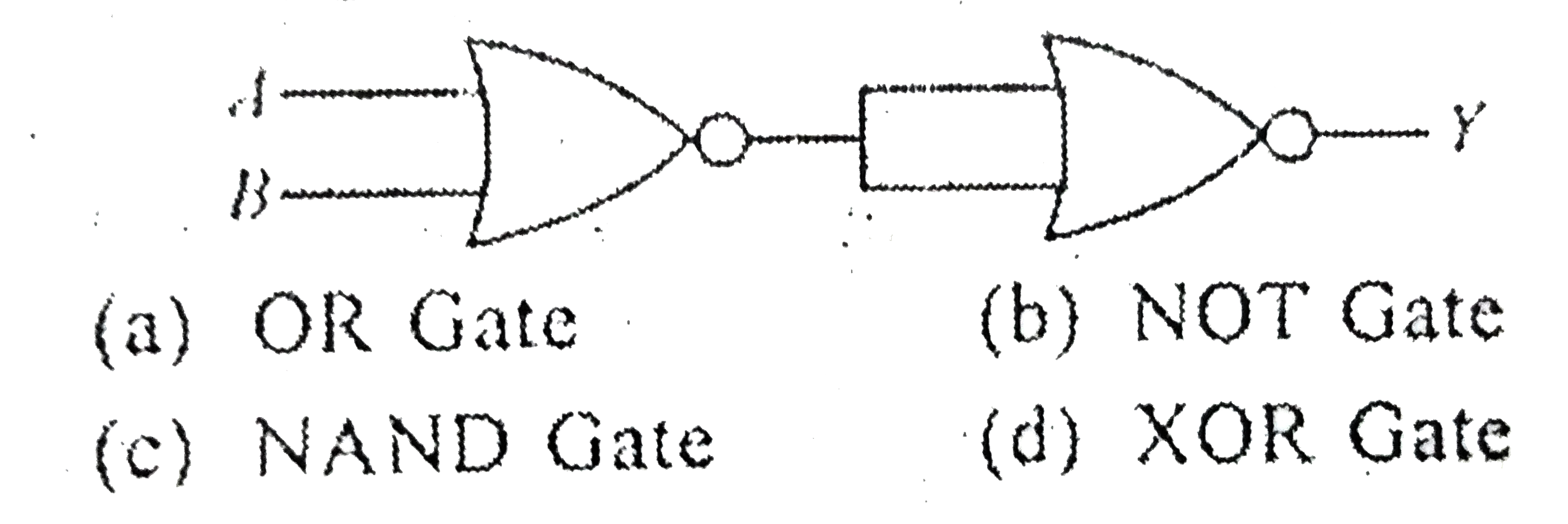
The logic gate represented in following figure is
 View Solution
The truth table for the following combination of gates is :-
_E01_430_Q01.png) View Solution
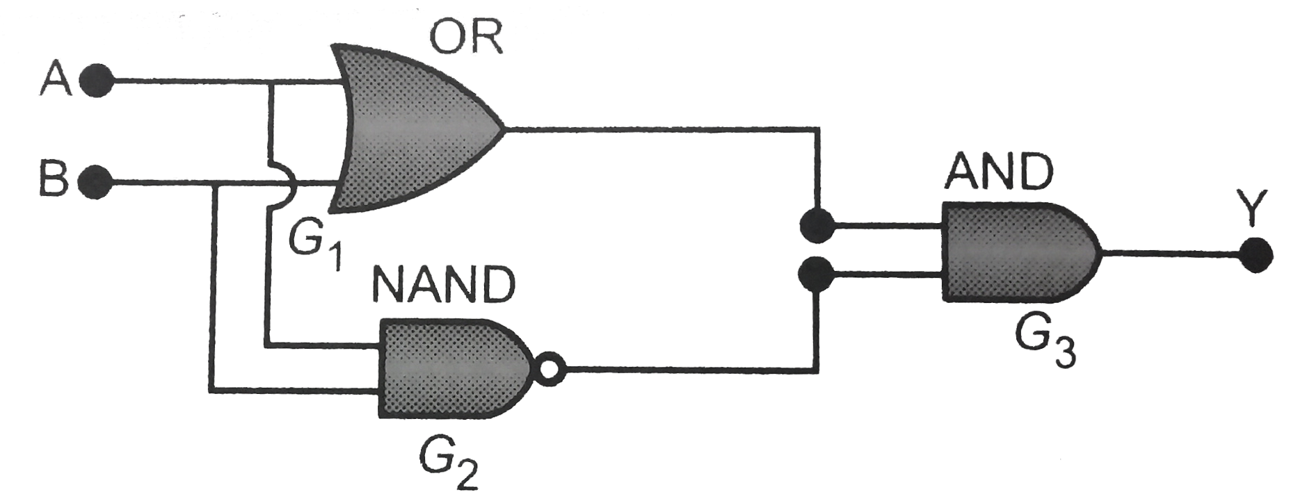
View SolutionThe following configuration of gate is equivalent to
 View Solution
The logic gate given below represents a
 View Solution
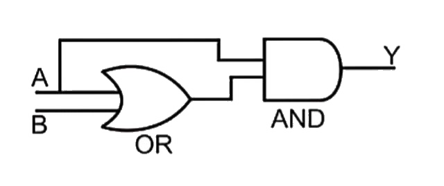
The output Y of the combination of logic gates shown is equal to
 View Solution
Which of the following represents NAND gate ?
View SolutionAn X-OR gate has following truth table:
It is represented by following logic relation
y=¯¯¯A.B+A.¯¯¯B
Build this gate using AND, OR and NOT gates.
∣∣ ∣ ∣ ∣ ∣ ∣∣ABY000011101110∣∣ ∣ ∣ ∣ ∣ ∣∣View SolutionWhich of the following gate is reversible
View Solution(a) In the figure given below the input waveform is converted into the output waveform by a device 'X'. Name the device and draw its circuit diagram.

(b) Identify the logic gate represented by the circuit as shown and write its truth table.
 View Solution
The combination of gates shown below yields
 View Solution

