Complete Solutions to Assertion Reason of chapter SEMICONDUCTOR ELECTRONICS of Class 12 book with complete answers and questions
| Class 12 | PHYSICS |
| Chapter | SEMICONDUCTOR ELECTRONICS |
| A2Z | Assertion Reason |
| Number Of Questions | 18 |
| Academic Year | 2023-24 |
Assertion: Microwave communication is preferred power optical communication.
Reason: Microwaves provide large number of channels and bandwidth compared to optical signals.
View SolutionAssertion: The resistivity of a semiconductor increases with temperature.
Reason: The atoms of a semiconductor vibrate with larger amplitude at higher temperature therby increasing it resistivity.
View SolutionAssertion: In a transistor the base is made thin.
Reason: A thin base makes the transistor stable.
View SolutionAssertion: A transistor amplifier is common emitter configuration has a low input impedence.
Reason: The base to emitter region is forward biased.
View SolutionAssertion: Diode lasers are used as optical sources in optical communication.
Reason: Diode layers consume less energy.
View SolutionAssertion: The logic gate `NOT` can be built using diode.
Reason: The output voltage and the input voltage of the diode have `180^(@)` phase difference.
View SolutionAssertion: The number of electrons in a `p`-type silicon semiconductor is less than the number of electrons ina pure silicon semiconductor at room temperature.
Reason: It is due to law of mass action.
View SolutionAssertion: Television signals are recieved throgh sky-wave propagation.
Reason: The ionosphere reflects em wave of frequencies greater than a critical frequency.
View SolutionAssertion: Em wave with frequencies more than the critical frequency of ionosphere cannot be used for communication using sky-wave propagation.
Reason: The refractive index of the ionosphere becomes very high for frequencies higher than the crtical frequency.
View SolutionAssertion: In common base configuration, the current gain of the transistor is less than unity.
Reason: The collector terminal is reverse biased for amplification.
View SolutionAssertion: A `p-n` junction with reverse biase can be used as a photo-diode to measure light intensity.
Reason: In reverse bias condition the current is small but it is more sensitive to change in incident light intensity.
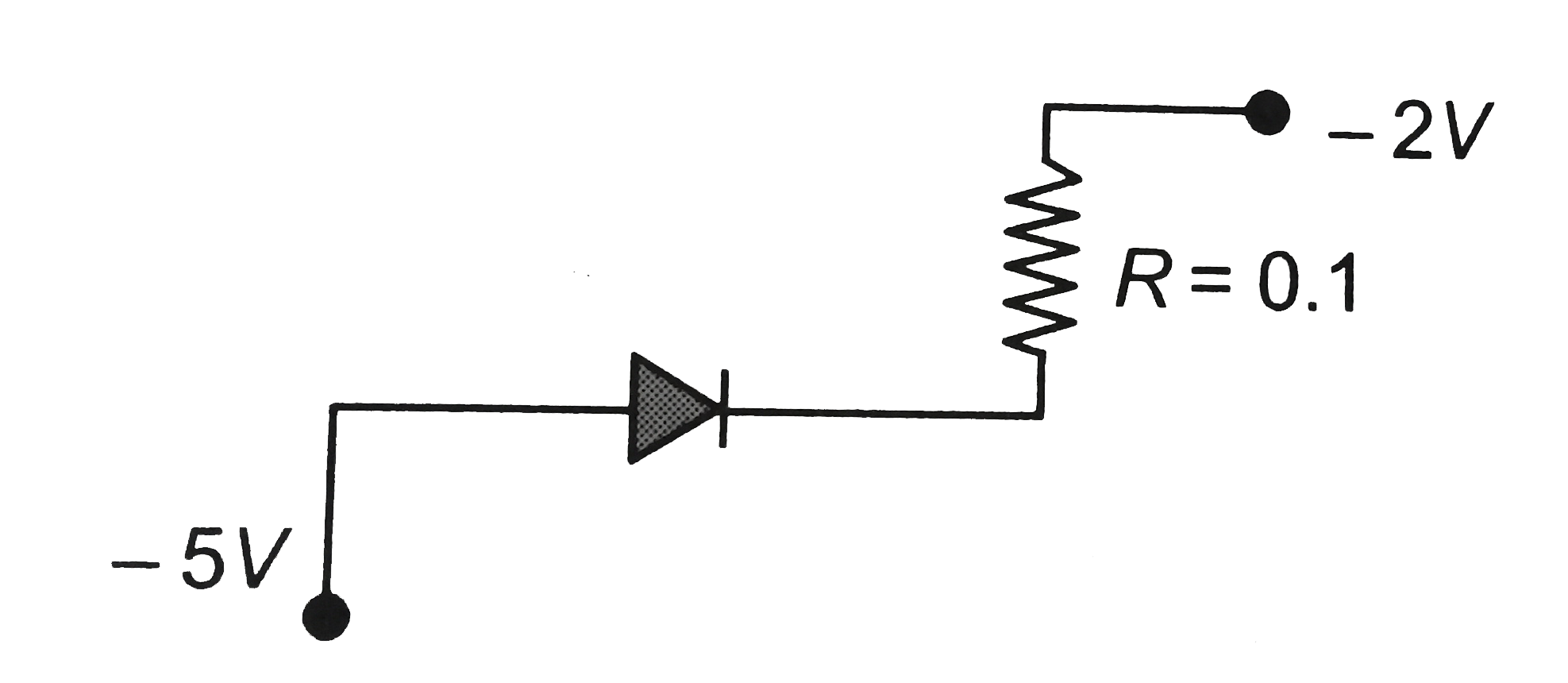
View SolutionAssertion : The value of current through `P - n` junction in the given figure will be `10 mA`.
Reason : In the above figure, p-side is at higher potential than n-side.

View SolutionAssertion:The dominant mechanism for motion of charge carriers in forward and reverse biased silicon `P-N` junction are drift in both forward and reverse biase.
Reason: In reverse biasing, no current flow through the junction.
View SolutionAssertion: The current gain in common base circuit is always less than one.
Reason: At constant collector votalge the change in collector current is more than the change in emitter current.
View SolutionAssertion: `NOT` gate is also called inverter circuit.
Reason: `NOT` gate inverts the input order.
View SolutionAssertion: In the following circuit the potential drop across the resistance is zero.

Reason: The given resistance has low value.
View SolutionAssertion: The following circuit represents `'OR'` gate

Reason: For the above circuit `Y=bar(X)=bar(bar(A+B))=A+B`
View SolutionAssertion : An `N`-type semiconductor has a large number of electrons but still it is electrically neutral.
Reason: An `N`-type semiconductor is obtained by doping an intrinsic semiconductor with a pentavelent impurity.
View Solution
Assertion Reason questions and complete solutions for chapter SEMICONDUCTOR ELECTRONICS of A2Z PHYSICS (HINGLISH) of Class 12