Complete Solutions to AIPMT/NEET Questions of chapter SEMICONDUCTOR ELECTRONICS of Class 12 book with complete answers and questions
| Class 12 | PHYSICS |
| Chapter | SEMICONDUCTOR ELECTRONICS |
| A2Z | AIPMT/NEET Questions |
| Number Of Questions | 77 |
| Academic Year | 2023-24 |
The intrinsic semiconductor becomes an insulator at
View SolutionThe truth table given below is for which gate?
`|(A,B,C),(0,0,1),(0,1,1),(1,0,1),(1,1,0)|`
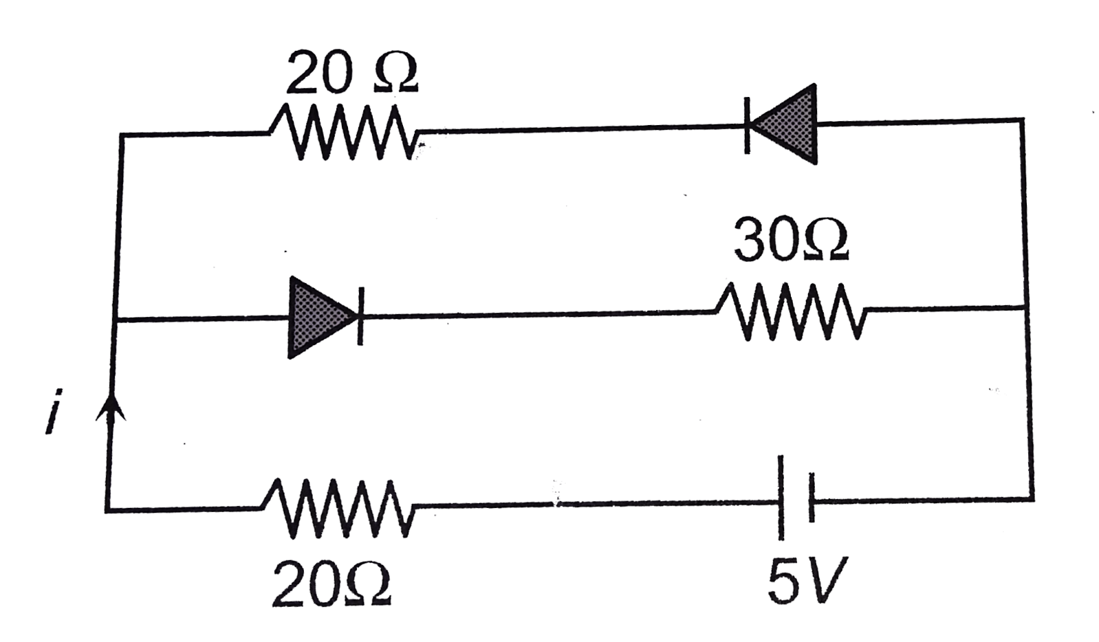
View SolutionCurrent in the circuit will be
View SolutionIn a `p-n` junction
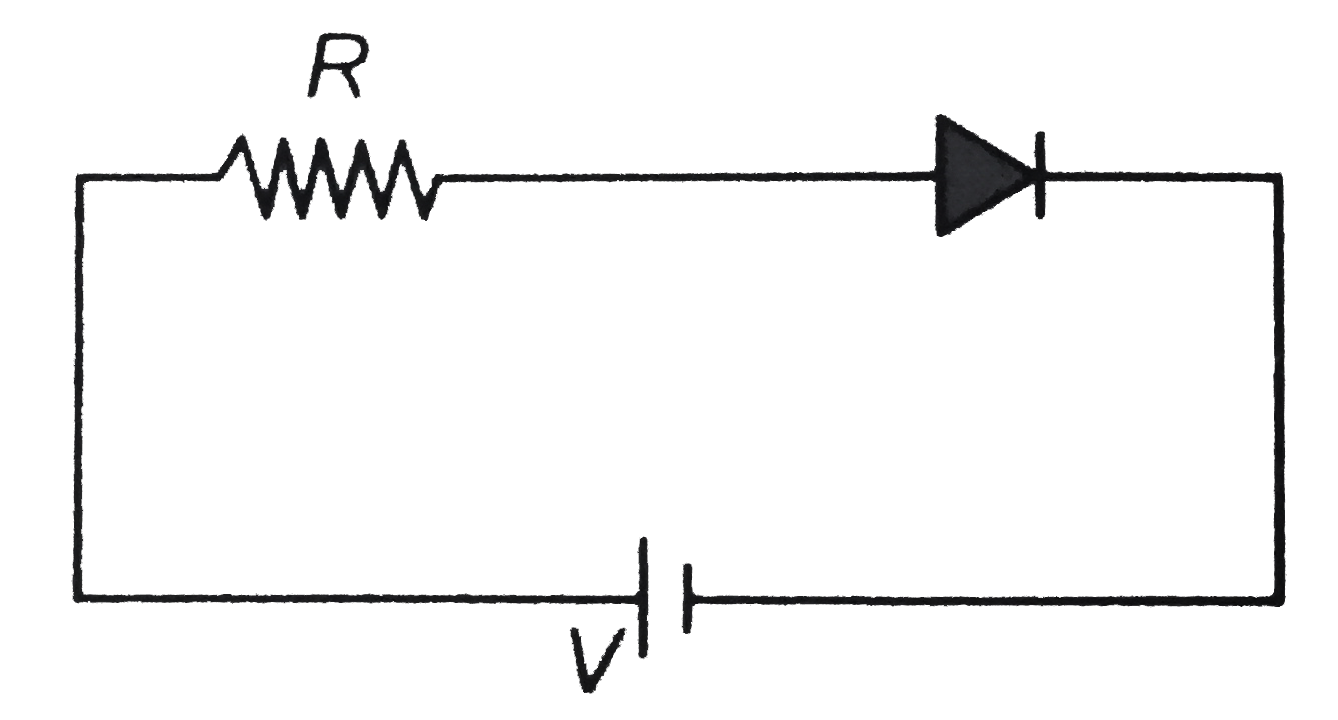
View SolutionFor the given circuit of `PN`-junction diode, which of the following statements is correct?
View SolutionFor a common base configuration of `PNP` transistor `(l_(C))/(l_(E))=0.98`, then maximum current gain in common emitter configuration will be
View SolutionThermionic emission from a heated filament varies with its temperature `T` as
View SolutionBarrier potential of a `p-n` junction diode does not depend on
View SolutionFollowing diagram perfoms the logic function of

View SolutionWhen phosphorus and antimony are mixed in germanium, then
View SolutionThe reverse biasing in a `PN` junction diode
View SolutionIf a full wave reactifier circuit is operating from `50 Hz` mains, the fundamental frequency in the ripple will be
View SolutionA `npn` transistor conducts when
View SolutionRegarding a semiconductor which one of the following statements is wrong?
View SolutionIn semiconductor at a room temperature
View SolutionThe peak voltage in the output of a half-wave diode rectifier fed with a sinusiodal signal without filter is `10 V`. The `dc` component of the output voltage is
View SolutionThe output of `OR` gate is `1`
View SolutionIn a `p-n` junction photo cell, the value of the of the photo electromotive force produced by monochromatic light is proportional to
View SolutionOf the diodes shown in the following diagrams, which one is reverse biased?
View SolutionChoose the only false statement form the following
View SolutionCarbon , silicon and germanium have four valence elcectrons each . These are characterised by valence and conduction bands separated by energy band - gap respectively equal to ` (E_g)_(c) (E_g)_(si) ` and ` (E_g)_(Ge) `. Which of the following statements ture ?
View SolutionApplication of a forward biase to a `p-n` junction:
View SolutionZenor diode is used for
View SolutionCopper has face centred cubic `(fc c)` lattice with interatomic spacing equal to `2.54 Å`. The value of the lattice constant for this lattice is
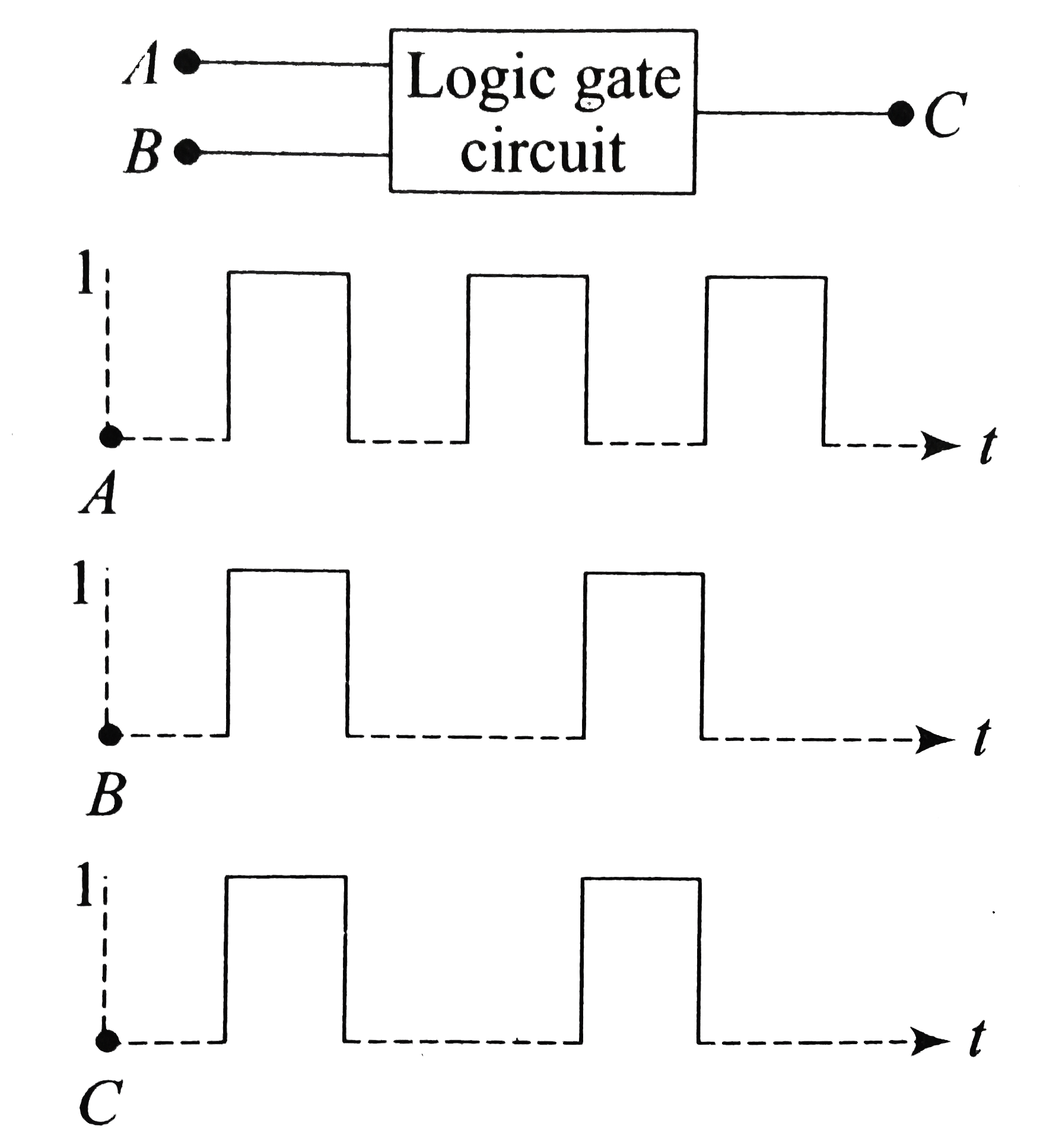
View SolutionThe following figure shows a logic gate circuit with two inputs `A` and `B` and the output `C`. The voltage waveforms of `A,B` and `C` are as shown below
View SolutionA transistor is operated in common emitter configuration at constant collector voltage `V_(c)=1.5 V` such that a change in the base current from `100 muA` to `150 muA` produces a change in the collector current from `5 mA` to `10 mA`. The current gain `(beta)` is
View SolutionA forward biased diode is
View SolutionThe radius of germanium `(Ge)` nuclide is measured to be twice the radius of `_(4)^(9)Be`. The number of nucleons in `Ge`
View SolutionIn the following circuit, the output `Y` for all possible inputs `A` and `B` is expressed by the truth table:

View SolutionA common emitter amplifier has a voltage gain of `50`, an input impedence of `100 Omega` and an output impedence of `200 Omega`. The power gain of the of the amplifier is
View SolutionFor a cubic crystal structure which one of the following relations indicating the cell characterstic is correct?
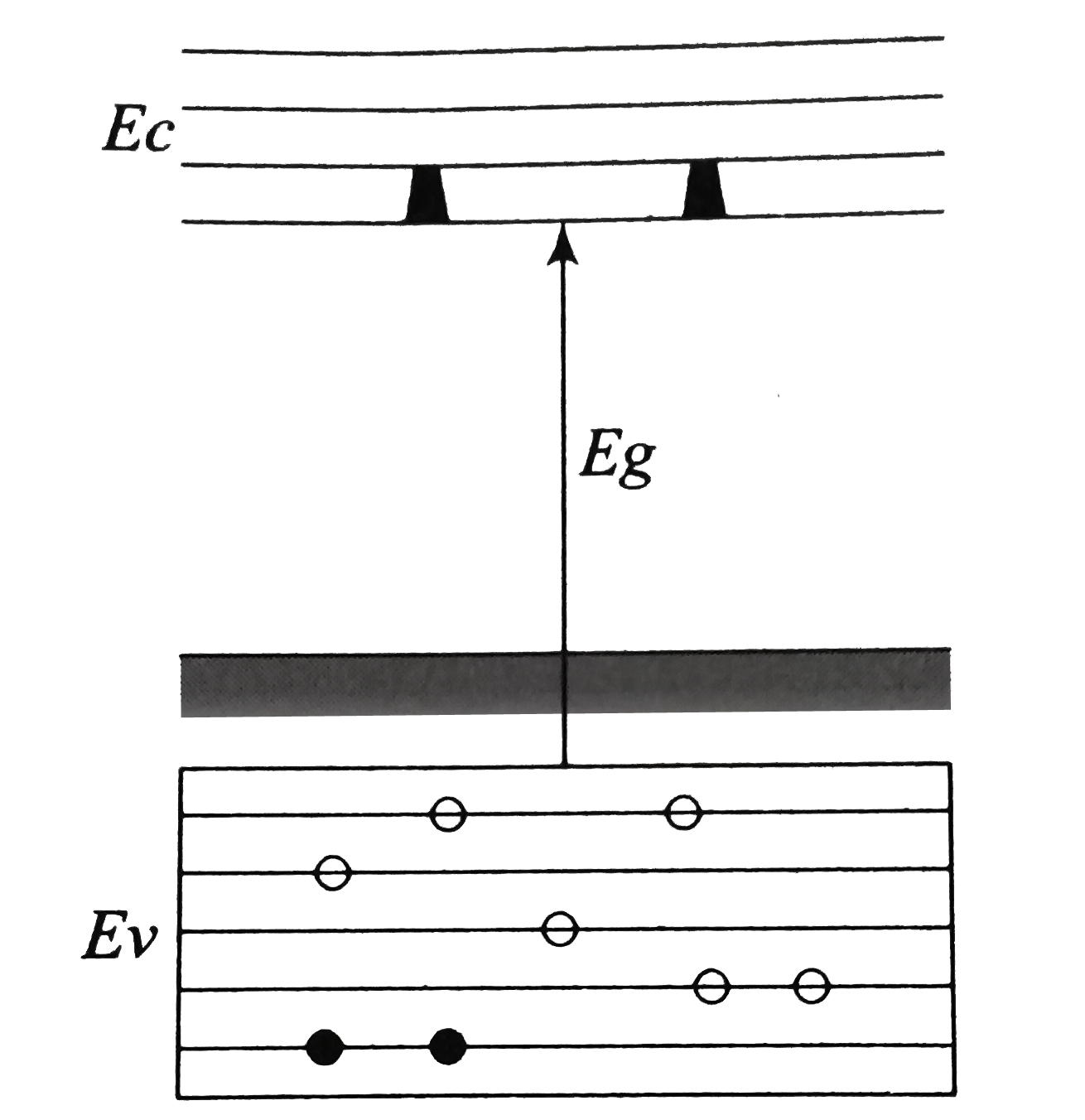
View SolutionIn the energy band diagram of a material shown below, the open circles and filled circles denote holes and electrons respectively. The material is a/an
View SolutionThe voltage gain of an amplifier with `9%` negative feedback is `10`. The voltage gain without feedback will be
View SolutionA `p-n` photodiode is made of a material with a band gap of `2.0 eV`. The minimum frequency of the radiation that can be absorbed by the material is nearly
View SolutionThe circuit is equivalent to

View SolutionA `p-n` photodiode is fabricated from a semiconductor with a band gap of `2.5 eV`. It can detect a signal of wavelength
View SolutionA transistor is operated in common emitter configuration at `V_(c)=2 V` such that a change in the base current from `100 muA` to `200 muA` produces a change in the collector current from `5 mA` to `10 mA`. The current gain is
View SolutionThe number of beta particles emitter by radioactive sustance is twice the number of alpha particles emitter by it. The resulting daughter is an
View SolutionSodium has body centred packing. Distance between two nearest atoms is `3.7 Å`. The lattice parameter is
View SolutionWhich one of the following statement is false?
View SolutionWhich one of the following bonds produces a solid taht reflects light in the visible region and whose electrical conductivity decreases with temperature and has high melting point?
View SolutionThe device that can act as a complete electronic circuit is
View SolutionIn order to obtain an output `Y=1` form the circuit of fig. the inputs must be
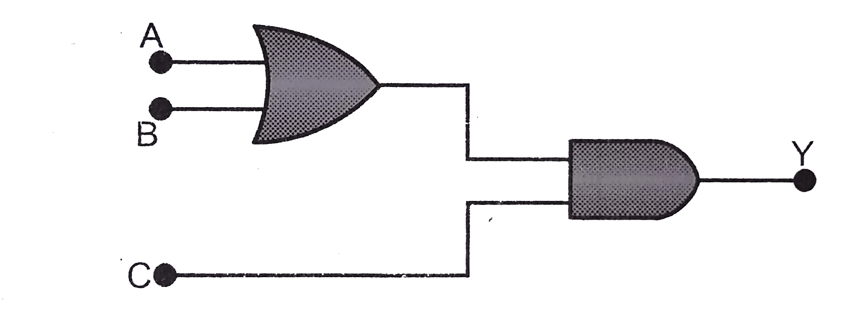
View SolutionA transistor is operated in common emitter configuration at `V_(c)=2 V` such that a change in the base current from `100 muA` to `300 muA` produces a change in the collector current from `10 mA` to `20 mA`. The current gain is
View SolutionIn forward bias, the width of potential barrier in a `P-N` junction diode
View SolutionSymbolic representation of four logic gates are shown as
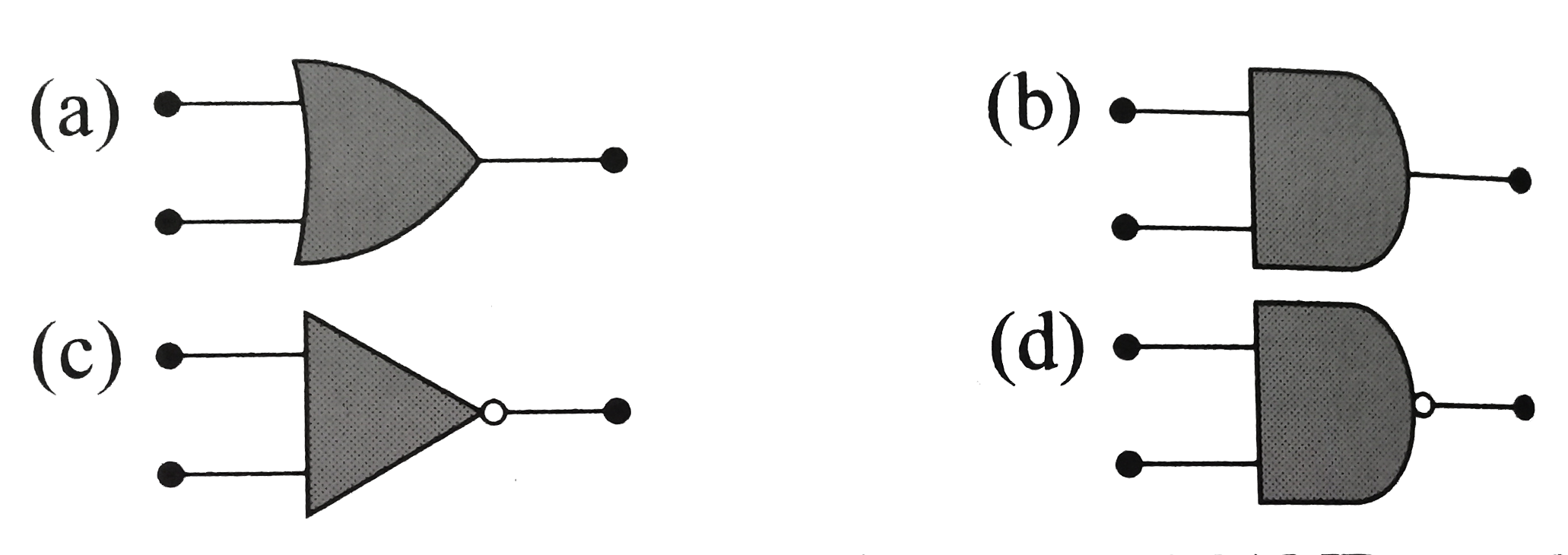
View SolutionIf a small amount of antimony is added to germanium crystal
View SolutionIn the following figure, the diodes, which are forward biased, are
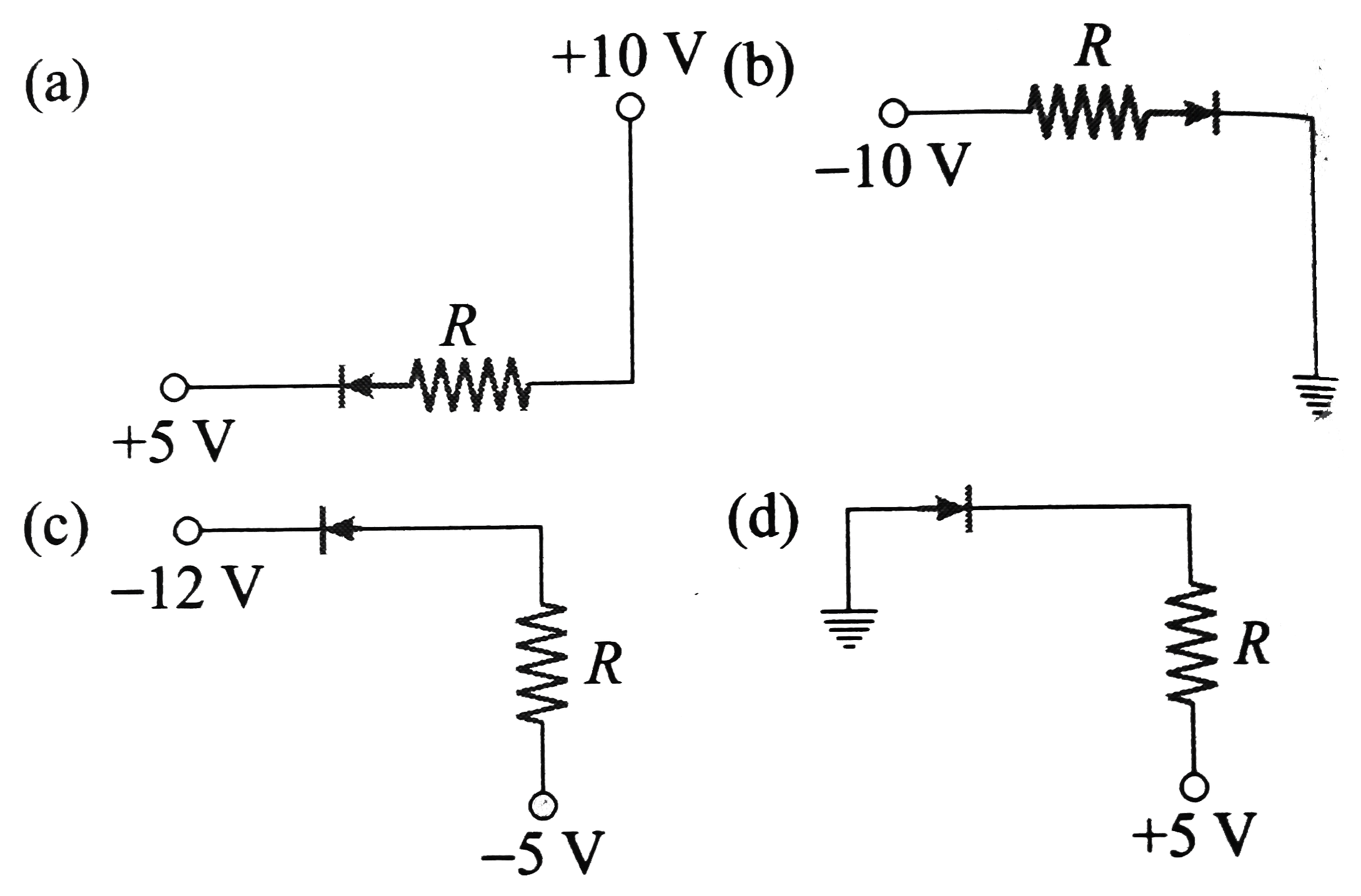
View SolutionPure `Si` at `500K` has equal number of electron `(n_(e))` and hole `(n_(h))` concentration of `1.5xx10^(16)m^(-3)`. Dopping by indium. Increases `n_(h)` to `4.5xx10^(22) m^(-3)`. The doped semiconductor is of
View SolutionA zener diode, having breakdown voltage equal to `15 V` is used in a voltage regulator circuit shown in the figure. The current through the diode is
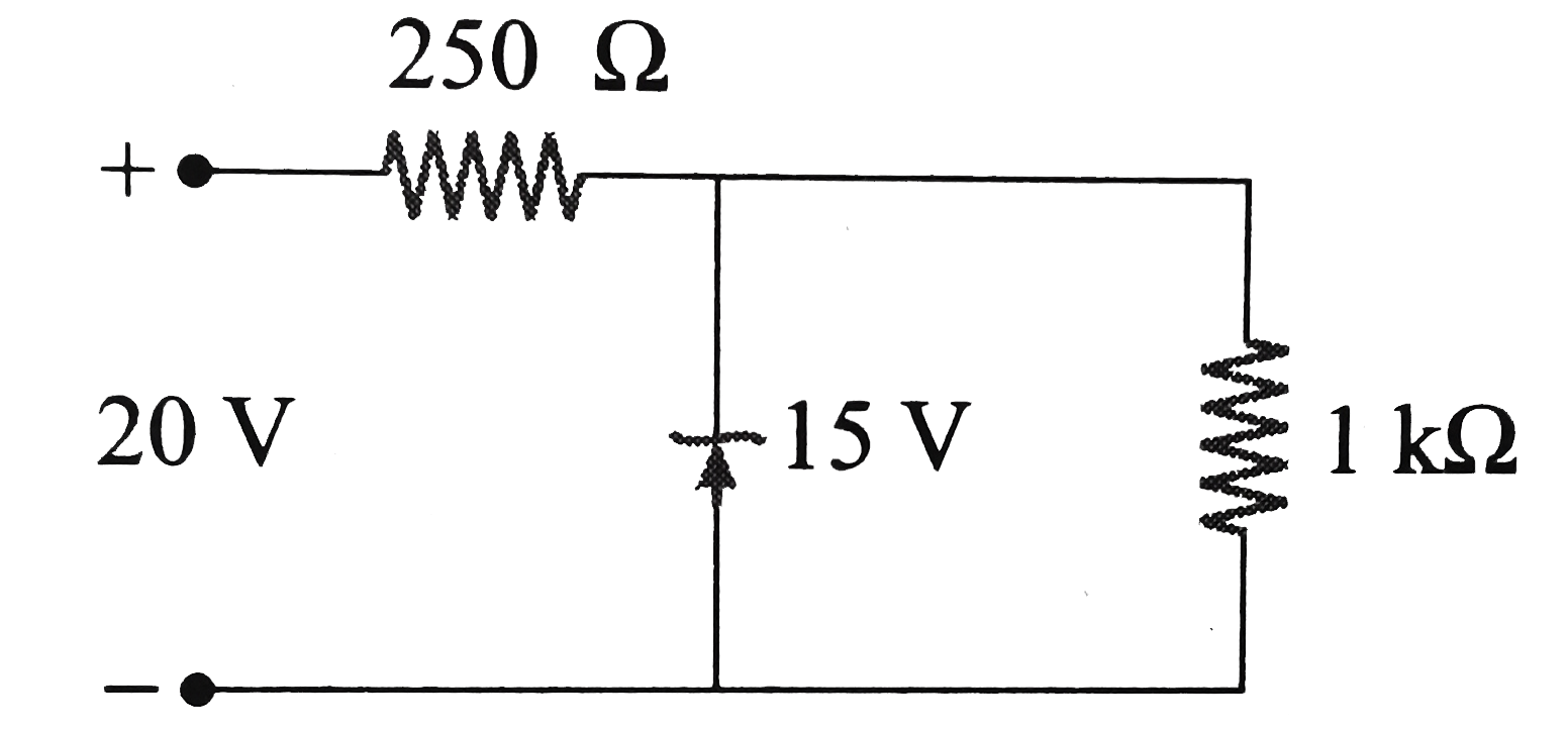
View SolutionTwo ideal diodes are connected to a battery as shown in the circuit. The current supplied by the battery is
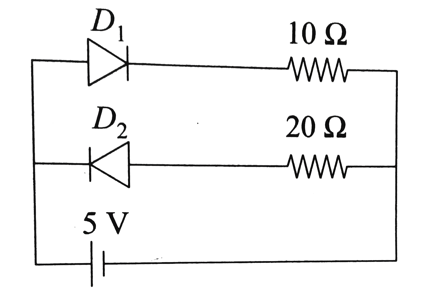
View SolutionIn a `CE` transistor amplifier, the audio signal voltage across the collector resistance of `2 k Omega` is `2 V`. If the base resistance is `1 k Omega` and the current amplification of the transistor is `100`, the input signal voltage is
View Solution`C` and `Si` both have same lattice structure, having `4` bonding electrons in each. However, `C` is insulator whereas `Si` is intrinsic semiconductor. This is because
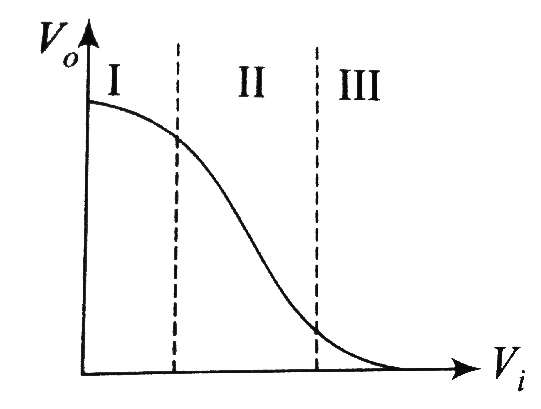
View SolutionTransfer characterstics [output voltage `(V_(o))` vs. input voltage `(V_(i))`] for a base biased transistor in `CE` configuration is as shown in the figure. For using transfor as a which, it is used
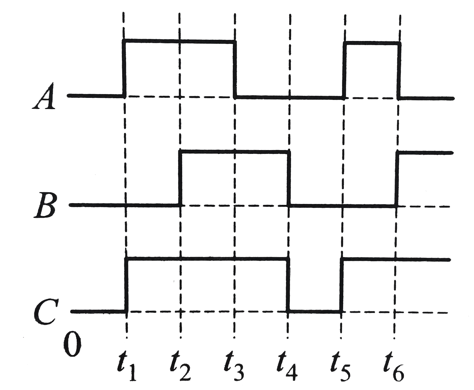
View SolutionThe figure shows a logic circuit with two inputs `A` and `B` and the output `C`. The voltage wave forms across `A,B` and `C` are as given. The logic circuit gate is
View SolutionThe input resistance of a silicon transistor is `100 Omega`. Base current is changed by `40 muA` which results in a change in collector current by `2 mA`. This transistor is used as a common-emitter amplifier with a load resistance of `4k Omega`. The voltage gain of the amplifier is
View SolutionIn order to obtain an output `Y=1` form the circuit of fig. the inputs must be

View SolutionIn a `n`-type semiconductor, which of the following statement is true?
View SolutionIn a common emitter `(CE)` amplifier having a voltage gain `G`, the transistor used has transconductance `0.03` mho and current gain `25`. If the above transistor is replaced with another one with transconductance `0.02` mho and current gain `20`, the voltage gain will be
View SolutionThe output `(X)` of the logic circuit shown in figure will be

View SolutionThe given graph represents `V-I` characterstic for a semiconductor device
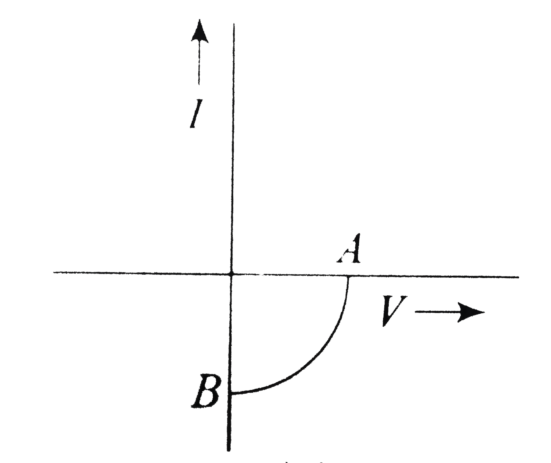
Which of the following satetement is correct?
View SolutionThe barrier potential of a `p-n`-junction depends on
(i) Type of semiconductor material
(ii) Amount of doping
(iii) Temperature which of the following is correct?
View SolutionWhich logic gate is represented by the following combination of logic gates ?

View SolutionIf an a `p-n`junction, a square input signal of `10V` is applied, as shown

then the output across `R_(L)` will be
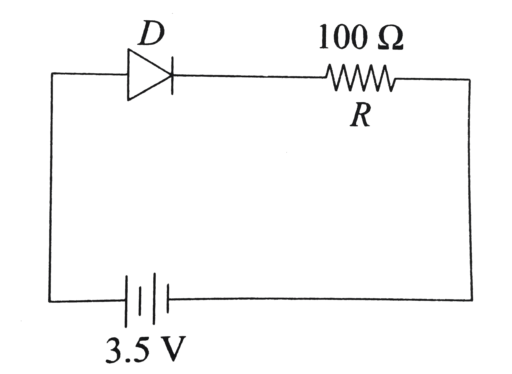
View SolutionIn the given figure, a diode `D` is connected to an external resistance `R=100 Omega` and an emf of `3.5 V`. If the barrier potential developed across the diode is `0.5 V`, the current in the circuit will be :
View SolutionConsider the junction diode as ideal. The value of current flowing throgh `AB` is:

View SolutionA `npn` transistor is connected in common emitter configuration in a given amplifier. A load resistance of `800 Omega` is connected in the collector circuit and the voltage drop across it is `0.8 V`. If the current amplification factor the voltage gain and the power gain of the amplifies will respectively be:
View SolutionTo get output `1`for the following circuit, the correct choice for the input is :

View SolutionFor `CE` transistor amlifier, the audio signal voltage across the collector resistance of `2 k Omega` is `4V`. If the currents amplification factor of the transistor is `100` and the base resistance is `1 k Omega`, then the input signal voltage is
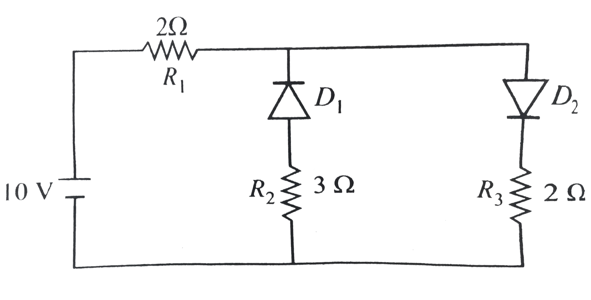
View SolutionThe given circuit has two ideal diodes connected as show in the figure. The current flowing through the resistance `R_(1)` will be
View SolutionWhat is the output `Y` in the following circuit, when all the three output `A,B,C` are first `0` and then `1`?

View SolutionIn a common emitter transistor amplifier the audio signal voltage across the collector is `3 V`. The resistance of collector is `3 kOmega`. If current gain is `100` and the base resistance is `2 kOmega`, the voltage and power gain of the amlifier is :
View SolutionThe given electrical network is equivalent to:

View SolutionWhich of the following represents forward biase diode?
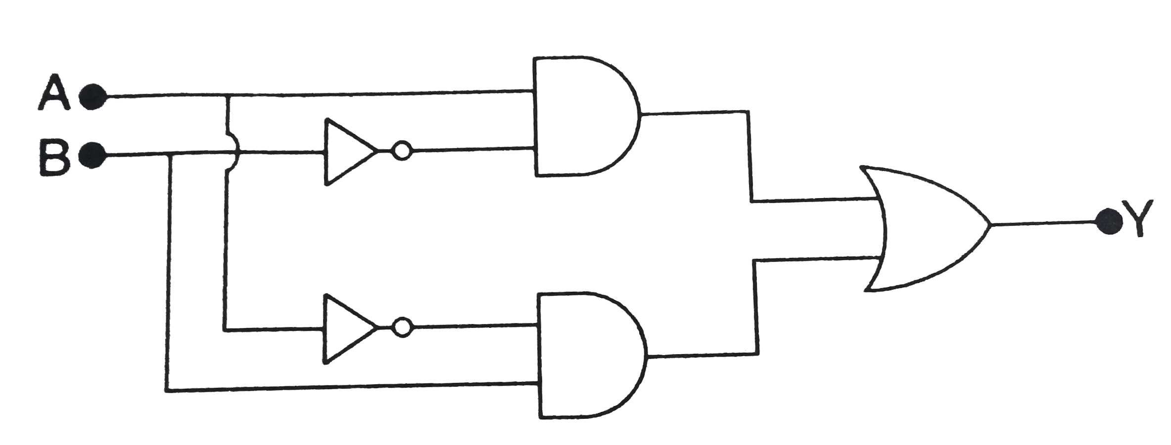
View SolutionIn the combination of the following gates the output `Y` can be written in terms of inputs `A` and `B` as:
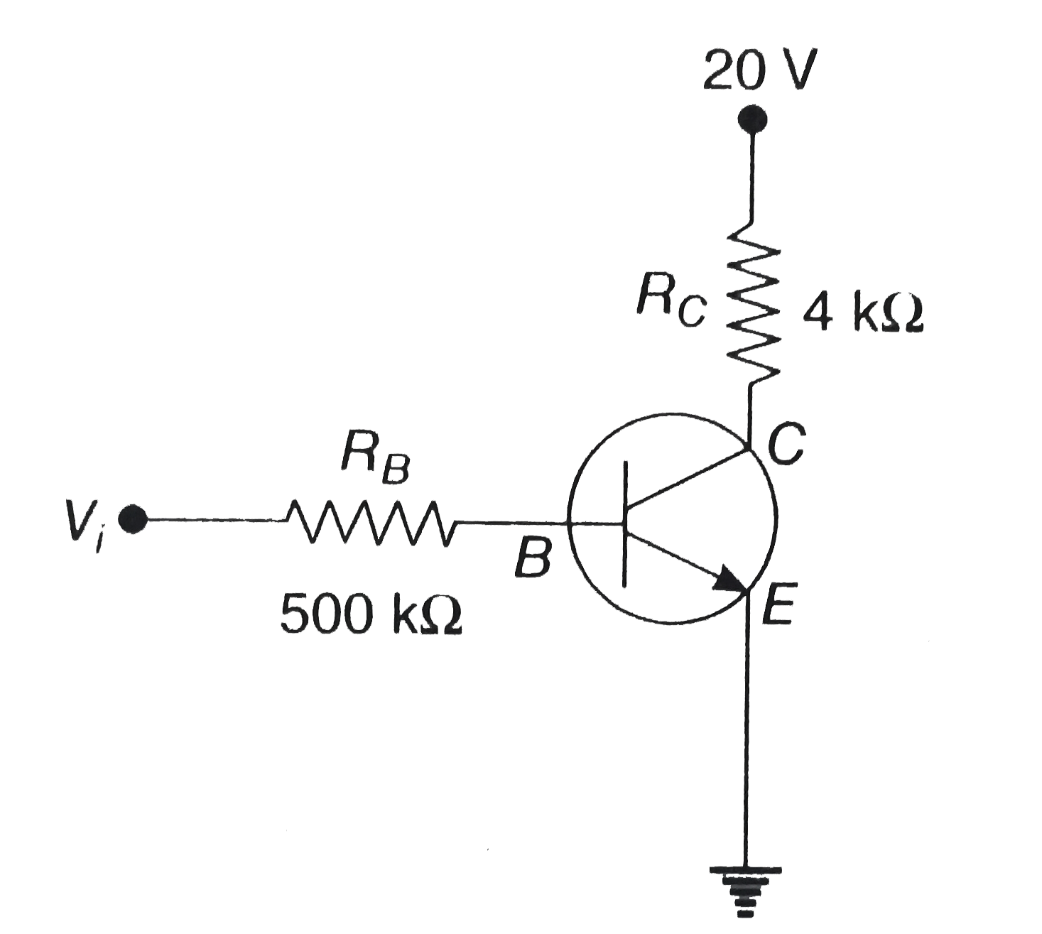
View SolutionIn the circuit shown in the figure, the input voltage `V_(i)` is `20V,V_(BE)=0` and `V_(CE)=0`. The values of `I_(B),I_(C)` and `beta` are given by:
View SolutionIn a `p-n` junction diode, change in temperature due to heating
View Solution
AIPMT/NEET Questions questions and complete solutions for chapter SEMICONDUCTOR ELECTRONICS of A2Z PHYSICS (HINGLISH) of Class 12