Complete Solutions to EXERCISE of chapter SEMICONDUCTOR ELECTRONICS of Class 12 book with complete answers and questions
| Class 12 | PHYSICS |
| Chapter | SEMICONDUCTOR ELECTRONICS |
| A2Z | EXERCISE |
| Number Of Questions | 29 |
| Academic Year | 2023-24 |
In a semiconductor,
View SolutionA peice of copper and the other of germanium are cooled from the room temperature to `80K`, then which of the following would be a correct statement?
View SolutionEnergy band in solids are a consequence of
View SolutionWhen forward bias is applied to a `P-N` junction, then what happence to the potential barrier `V_(B)`, and the width of charge depleted region `x`?
View SolutionWhen npn transistor is used as an amplifler
View SolutionFor a transistor ampliflier in common emiter configuration for load imperdance of `1 k Omega (h_(fe) = 50 and h_(oe) = 25)` the current gain is
View SolutionIf a full wave reactifier circuit is operating from `50 Hz` mains, the fundamental frequency in the ripple will be
View SolutionIn a common base ampifier , the phase difference between the input signal and output voltage is
View SolutionTo obtain a `P`-type `Si` semiconductor, we need to dope pure `Si` with
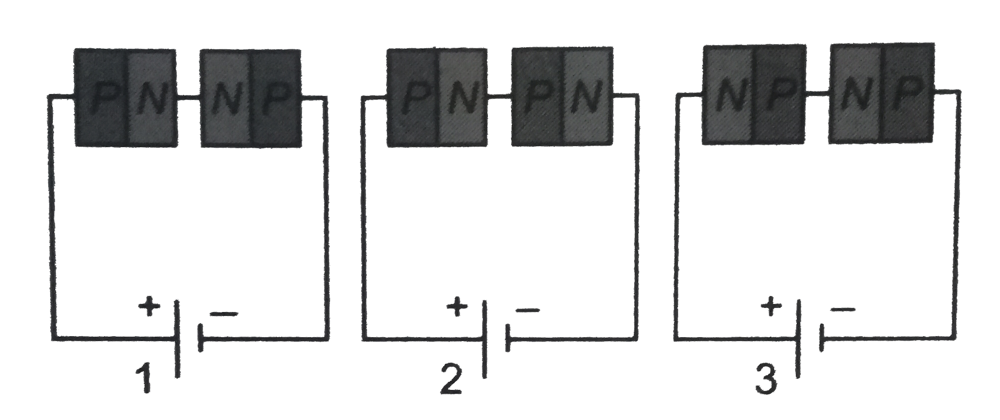
View SolutionTwo `PN`-junction can be connected in series by three different methods as shown in the figure. If the potential difference in the junction is the same, then the correct connection will be
View SolutionIn a p- n junction diode not connected to any circuit,
View SolutionWhich of the following statements is not true?
View SolutionThe dominant mechanisms for motion of charge carriers in forward and reverse biased silicon `P-N` junction are
View SolutionFor a given plate voltage , the plate current in a triode valve is maximum when the potential of
View SolutionThe probbility of electrons to be found in the conduction band of an intrinsit semiconductor at a finile temperature
View SolutionThe typical ionisation energy of a donor in silicon is
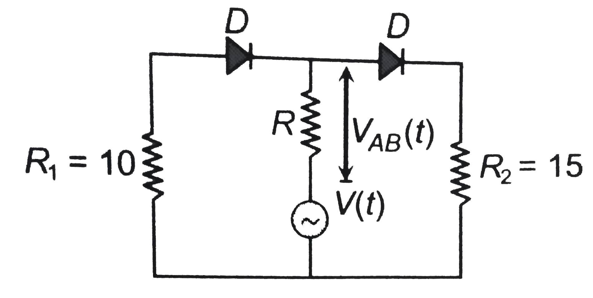
View SolutionIn the circuit given below, `V(t)` is the sinusoidal voltage source, voltage drop `V_(AB)(t)` across the resistance `R` is
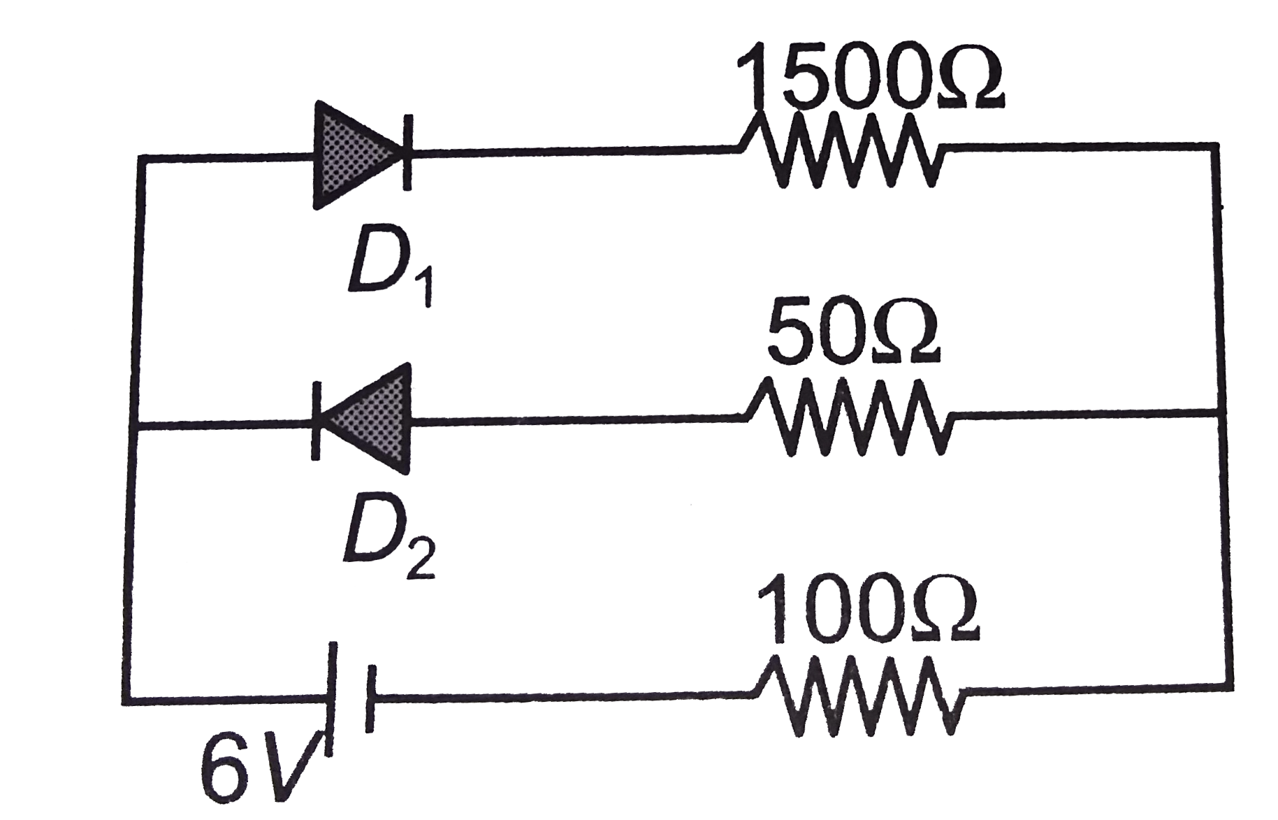
View SolutionThe circuit shown in following figure contanis two diode `D_(1)` and `D_(2)` each with a forward resistance of `50 ohm` and with infinite backward resistance. If the battery voltage is `6V`, the current through the `100` ohm resistance (in amperes) is
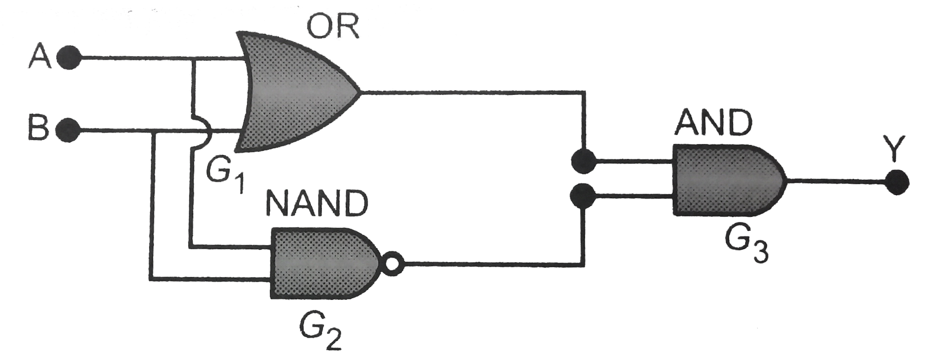
View SolutionThe following configuration of gate is equivalent to
View SolutionThe output of a `NAND` gate is `0`
View SolutionWe are accustomed to decinnial form of stating numbers. For example `127` stands for `100+20+7`. There is a binary from of numbers, useful in computers. Here `1011` stands for `8+0+2+1`. The binary from for decimal number `45` will be
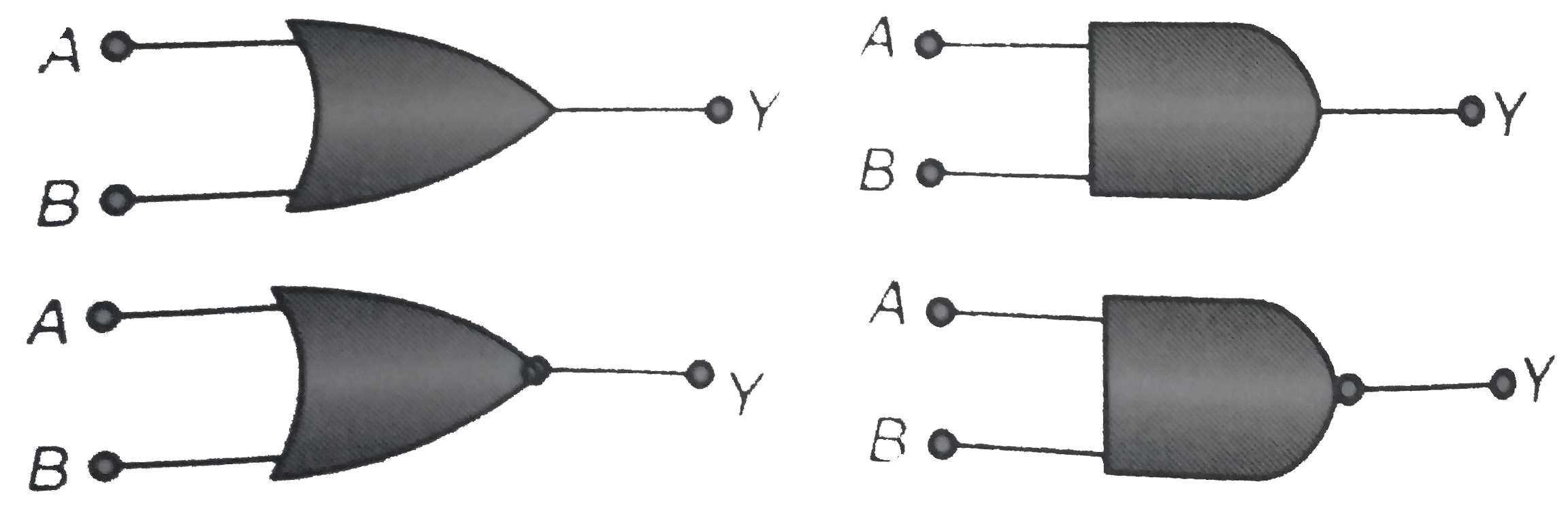
View SolutionGiven below are four logic tage symboles. Those for `OR, NOR` and `NAND` are respectively:
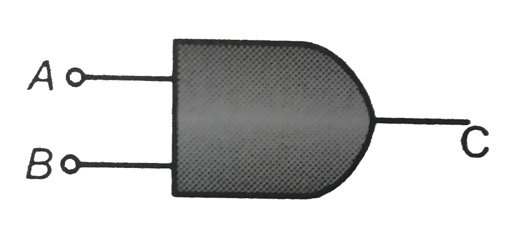
View SolutionConsider a two -input `AND` gate of figure. Out of the four entries for the truth. Table given here, the correct ones are
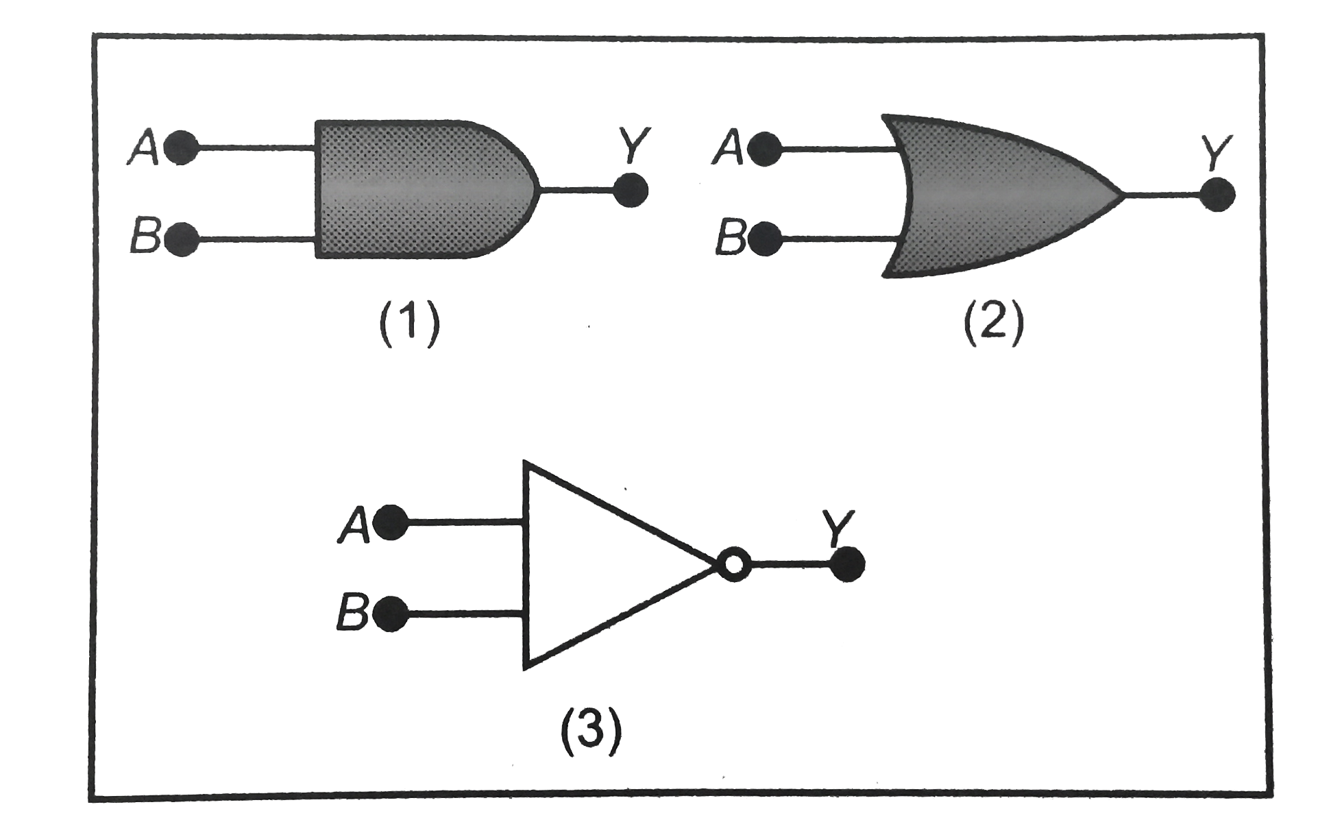
View SolutionGiven below are symbols for some gates. The `OR` gate and the `AND` gate, respectively are
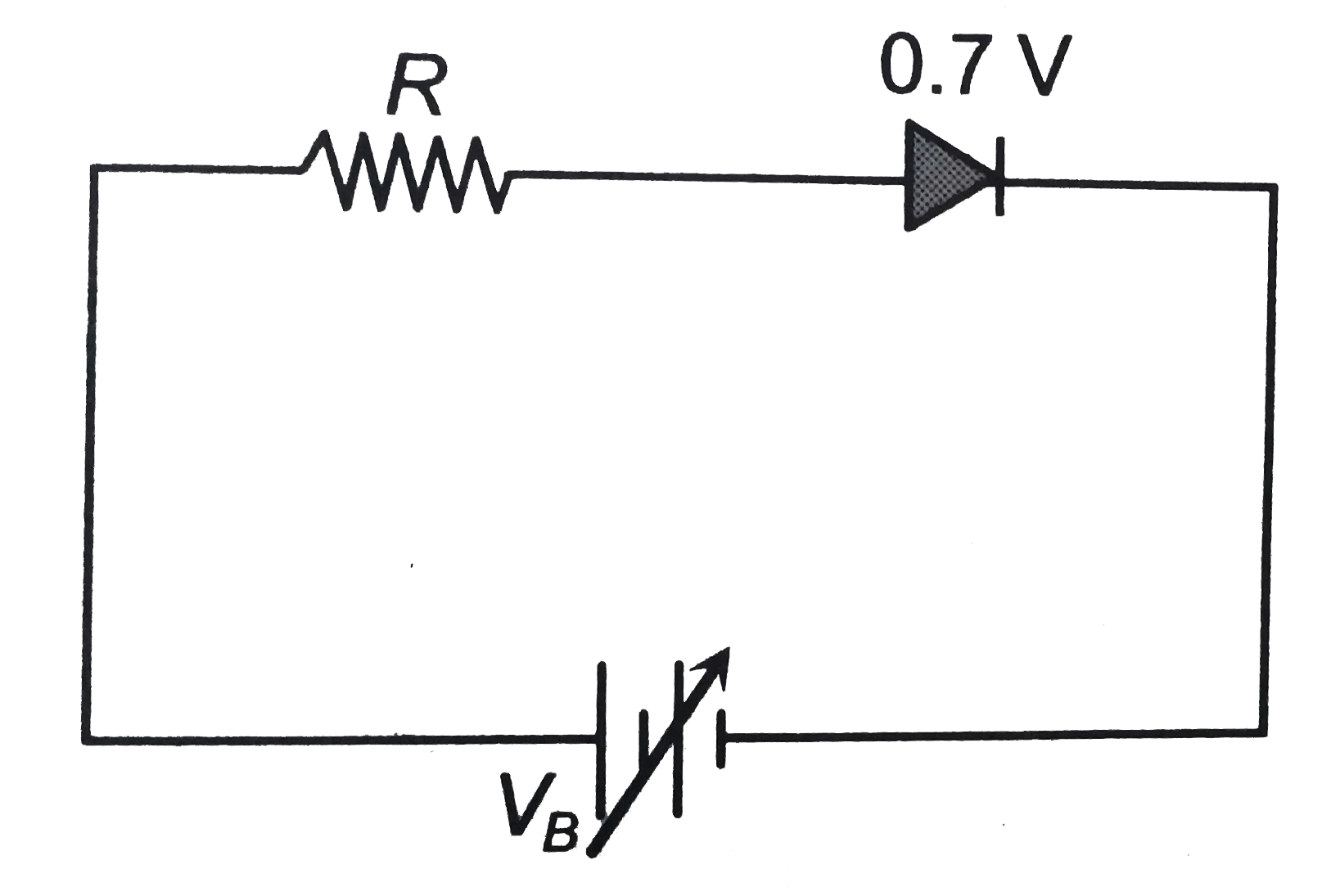
View SolutionThe junction diode in the following circuit requires a minimum current of `1 mA` to be above the knee point `(0.7 V)` of its `I-V` characterstic curve. The voltage across the diode is independent of current above the knee point. If `V_(B)=5 V`, then the maximum value of `R` so that the voltage is above the knee point, will be
View SolutionIn a silicon transistor, the base current is changed by `20 muA`. This results in a change of `0.02 V` in base to emitter voltage and a change of
View SolutionAssertion: We can measure the potential barrier of a `PN` junction by putting a sensitive voltmeter across its terminals.
Reason: The current through the `PN` junction is not same in forward and reversed bias.
View SolutionAssertion: Semiconductor do not obey Ohm's law.
Reason: Current is dertemined by the rate of flow of charge carriers.
View SolutionAssertion: In a transistor amplifier, the output voltage is always out of phase with the input voltage.
Reason: The emitter base junction is reverse biased and the base collector junction is forward biased.
View Solution
EXERCISE questions and complete solutions for chapter SEMICONDUCTOR ELECTRONICS of A2Z PHYSICS (HINGLISH) of Class 12