Complete Solutions to Digital Electronics of chapter SEMICONDUCTOR ELECTRONICS of Class 12 book with complete answers and questions
| Class 12 | PHYSICS |
| Chapter | SEMICONDUCTOR ELECTRONICS |
| A2Z | Digital Electronics |
| Number Of Questions | 40 |
| Academic Year | 2023-24 |
Which logic gate is represented by following diagram?

View SolutionSymbol

represented
View SolutionWhich gate is represented by this figure?

View SolutionIdentify the gate from the following

View SolutionWhich of the following is not correct?
View SolutionThe following configuration of gates is equivalent to
View SolutionIn the Boolean algebra `bar((bar(A).bar(B))). A` equal to
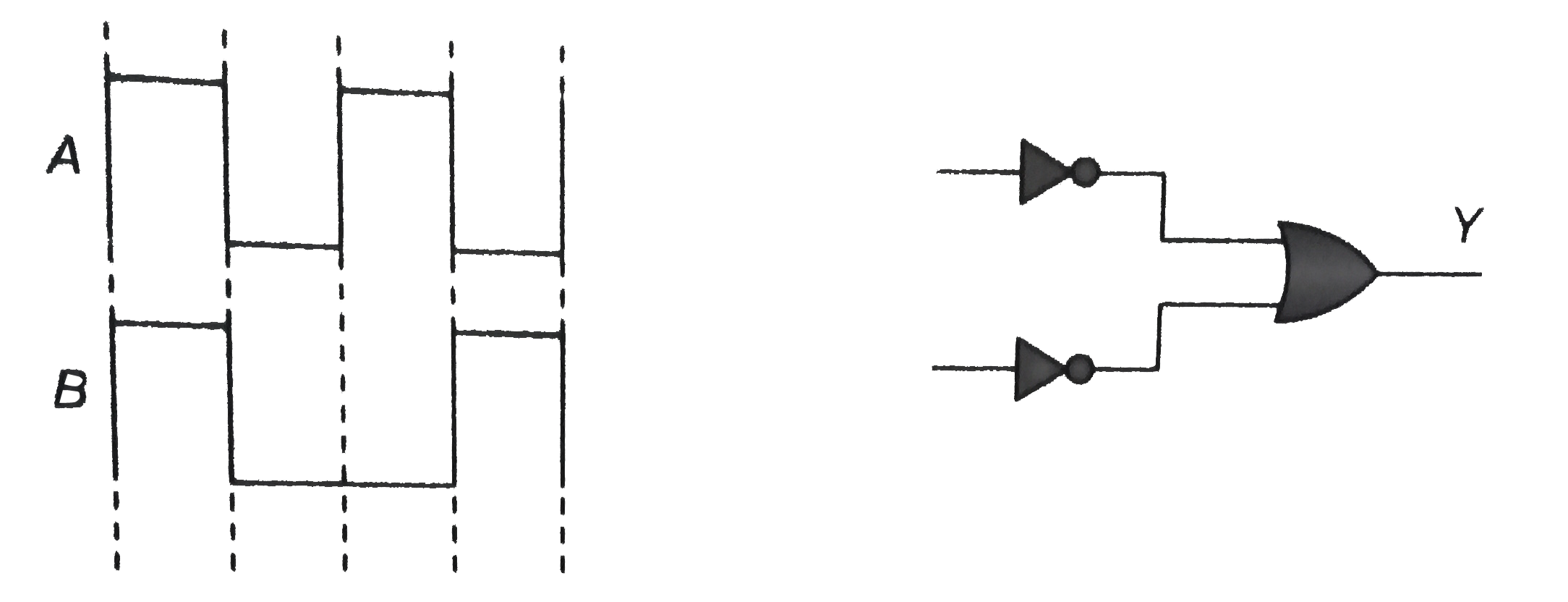
View SolutionIn the given circuit as shown the two input waveform `A` and `B` are applied simultaneously. The resultant waveform `Y` is
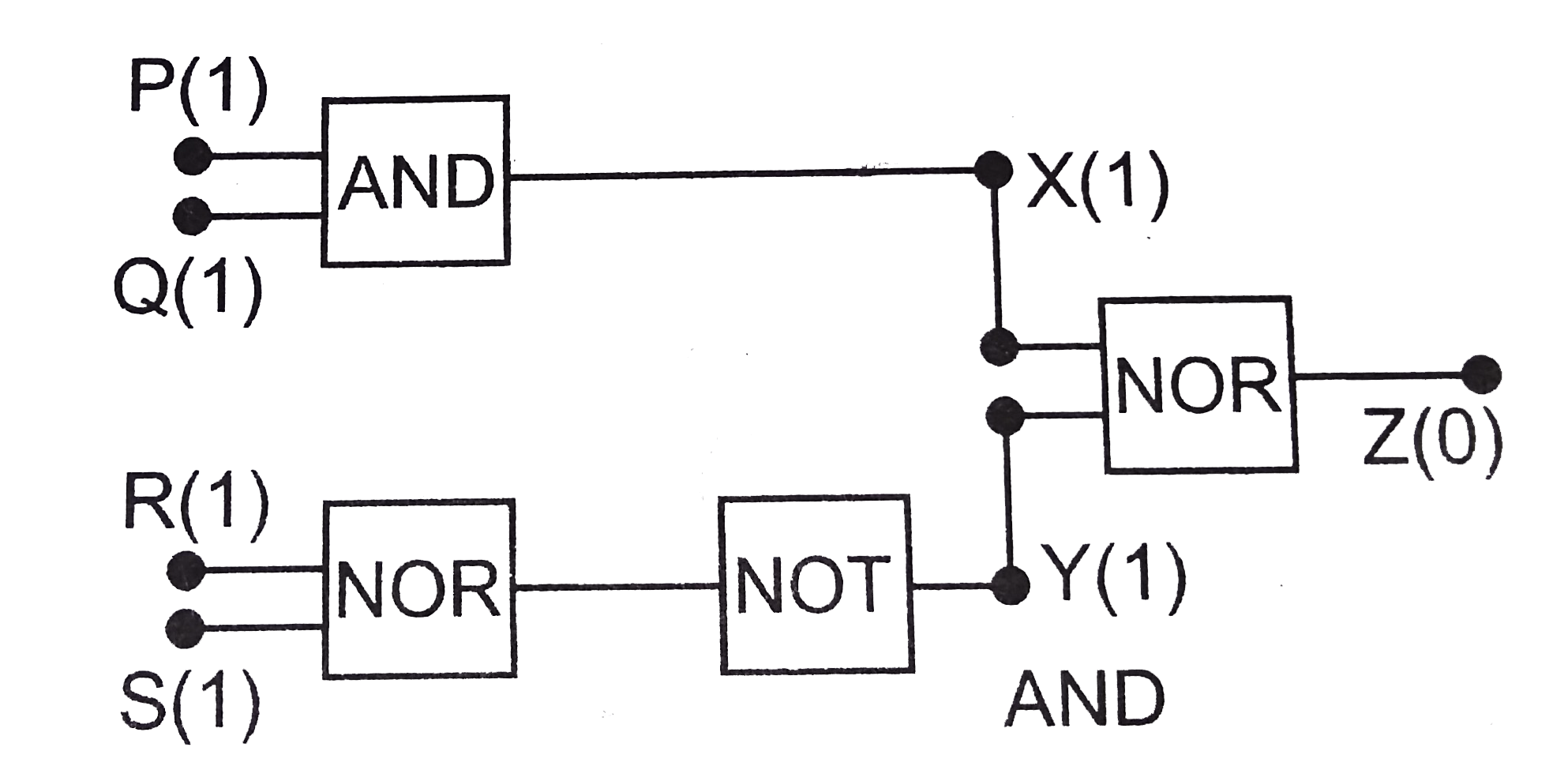
View SolutionThe circuit diagram (see fig.) shows a 'logic combination' with the states outputs `X,Y` and `Z` given for input `P,Q,R` and `S` all at state `1` (i.e., high). When inputs `P` and `R` change to state `0` i.e., low) with inputs `Q` and `S` still at `1`, the condition of output `X,Y` and `Z` chages to
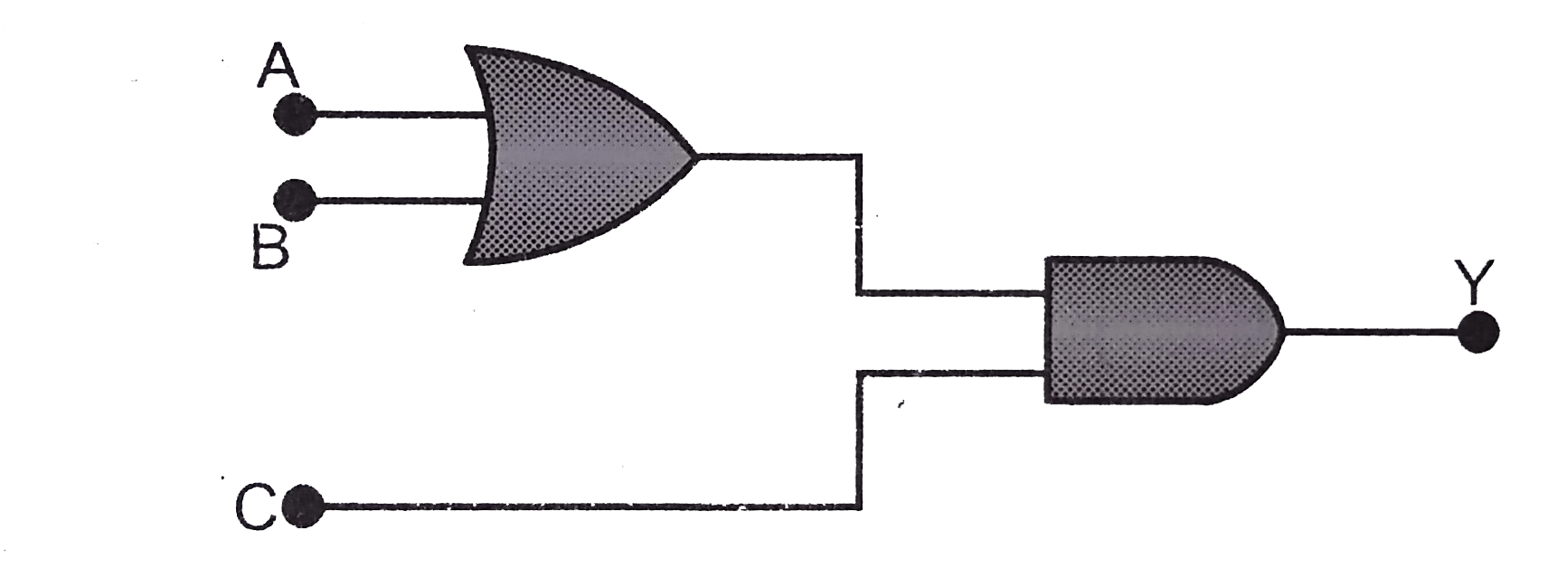
View SolutionIn order to obtain an output `Y=1` form the circuit of fig. the inputs must be
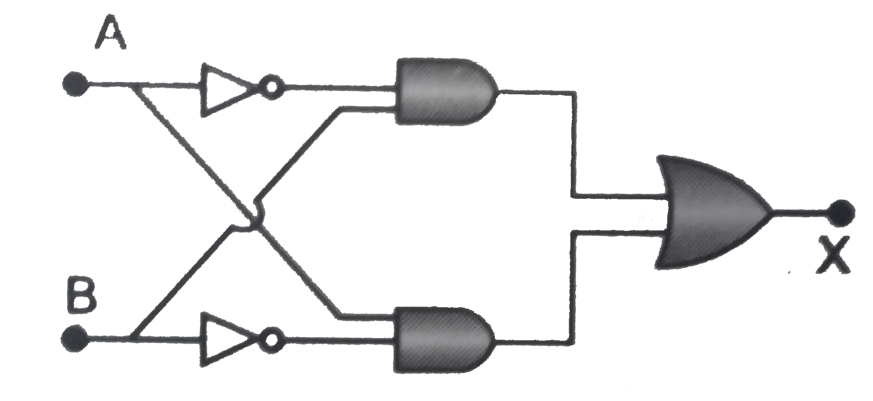
View SolutionWith reference to figure, which of the following is possible?
View SolutionName the Gate represented by the following circuit.

View SolutionThe following truth table corresponds to the logic gate
`|(A,0,0,1,1),(B,0,1,0,1),(X,0,1,1,1)|`
View SolutionThe combination of `'NAND'` gates shown here under (figure) are equivalent to
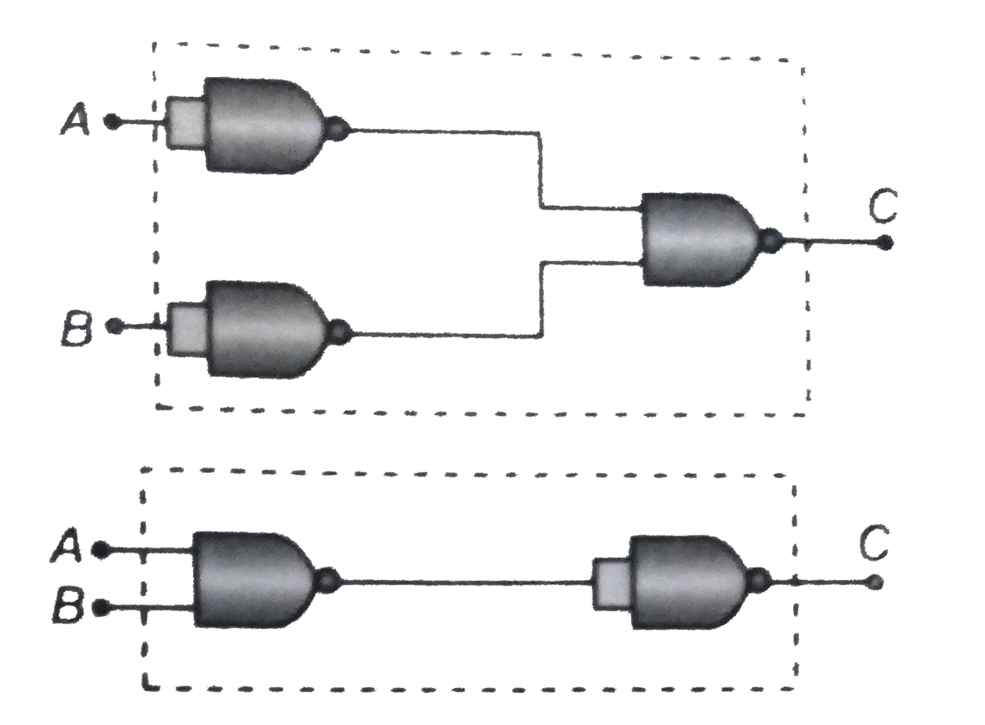
View SolutionThe following truth table corresponds to the logic gate
`|(A,B,X),(0,0,0),(0,1,1),(1,0,1),(1,1,1)|`
View SolutionWhich of the following gates corresponds to the truth table given below ?
`|(A,B,X),(1,1,0),(1,0,1),(0,1,1),(0,0,1)|`
View SolutionHow many `NAND` gate are used to from `AND` gate?
View SolutionThe following truth table belongs to which one of the following four gates?
`|(A,B,C),(1,1,0),(1,0,0),(0,1,0),(0,0,1)|`
View SolutionThe truth table given below is for:
`|(A,B,X),(0,0,0),(0,1,0),(1,0,0),(1,1,1)|`
View SolutionThe truth table given below is for which gate?
`|(A,B,C),(0,0,1),(0,1,1),(1,0,1),(1,1,0)|`
View SolutionGiven below are four logic tage symboles. Those for `OR, NOR` and `NAND` are respectively:
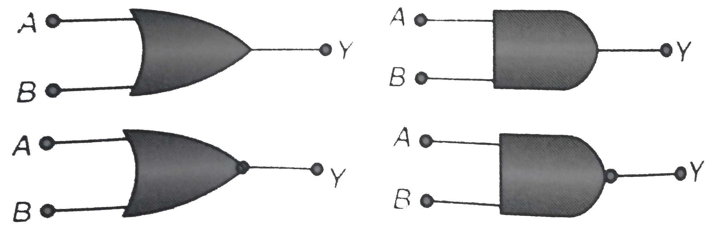
View SolutionWhich of the following gates will have an output of `1`?
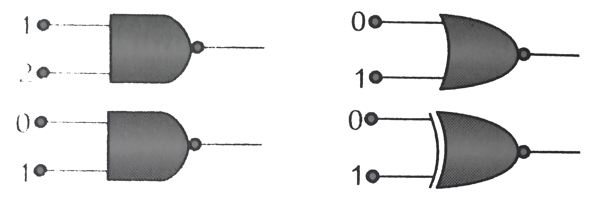
View SolutionA truth table is given below. Which of the following has this types fo truth table?
`|(A,0,1,0,1),(B,0,0,1,1),(Y,1,0,0,0)|`
View SolutionThe truth table shown in figure is for
`|(A,0,0,1,1),(B,0,1,0,1),(Y,1,0,0,1)|`
View SolutionFor the given combination of gates, if the logic states of inputs `A,B,C,` are as follows `A=B=C=0` and `A=B=1, C=0` then the logic states of output `D` are

View SolutionThe logic behind `'NOR'` gate is that it gives
View SolutionHow many `NAND` gate are used to from `AND` gate?
View SolutionWhich of the following gates will have an output of `1`?
View SolutionWhich of these represents `NAND` gate?
View SolutionThe given truth table is of
`|(A,X),(0,1),(1,0)|`
View SolutionWhat will be the input of `A` and `B` for the Boolean expression `bar((A+B)).bar((A.B))=1`?
View SolutionIf `A` and `B` are two inputs in `AND` gate, then `AND` gate has an output of `1` when the values of `A` and `B` are
View SolutionIn order to obtain an output `Y=1` form the circuit of fig. the inputs must be

View SolutionThe combination of the gates shown in the figure below produces
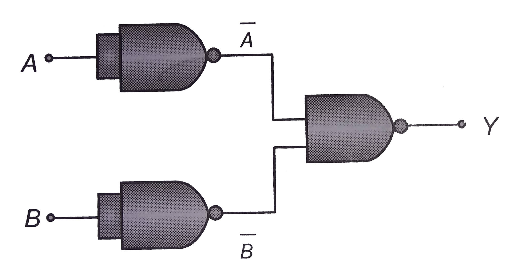
View SolutionSum of the two binary numbers `(1000010)_(2)` and `(110011)_(2)` is
View SolutionFigure gives a system of logic gates. From the study of truth table it can be found that no produce a high output `(1)` at `R`, we must have
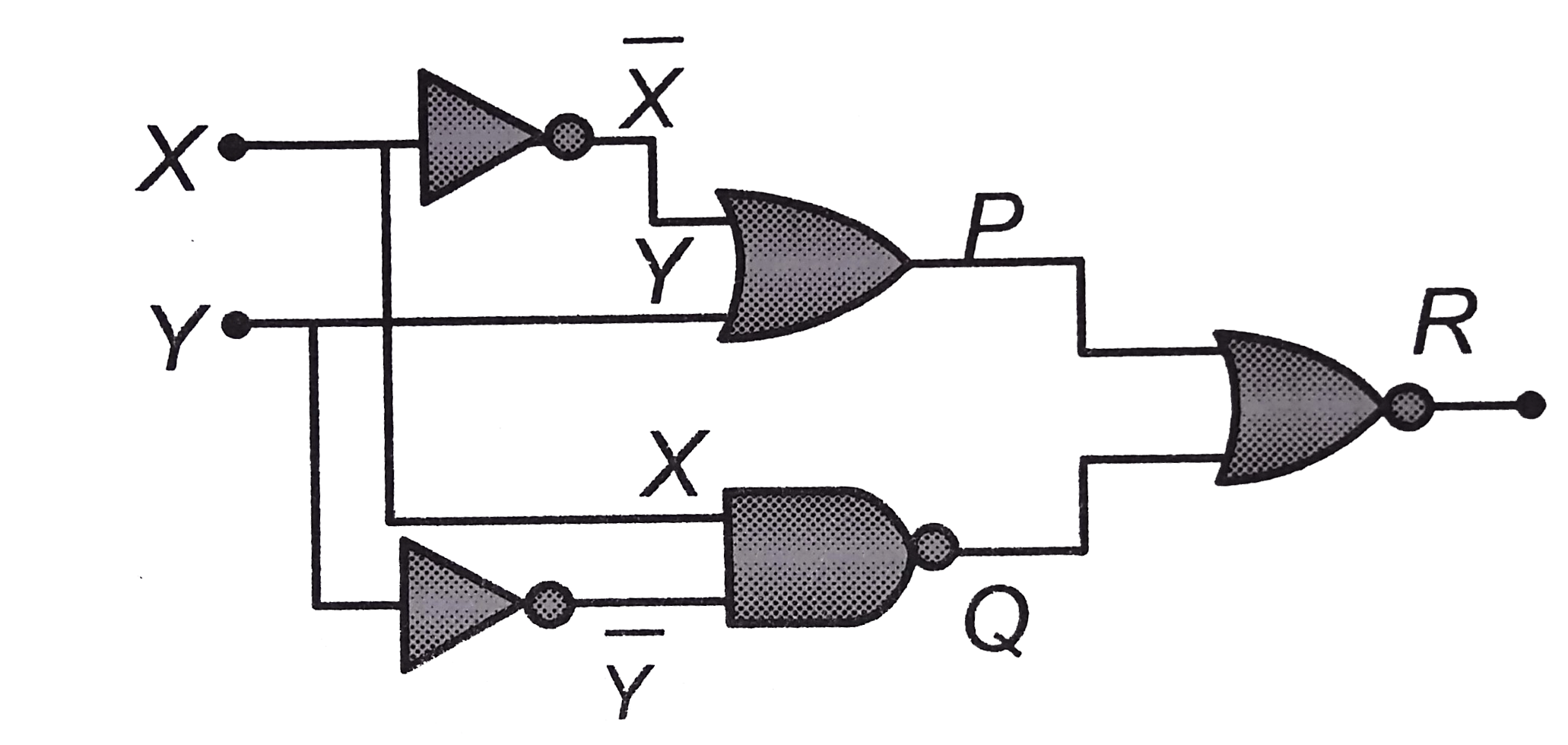
View SolutionThe combination of gates shown below produces
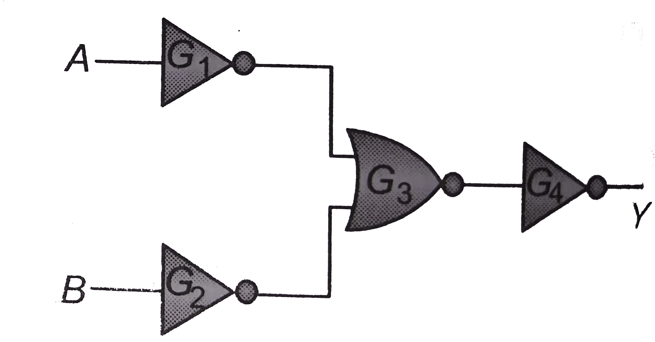
View SolutionThe figure shows two `NAND` gates followed by a `NOR` gate. The system is equivalent to the following logic gate
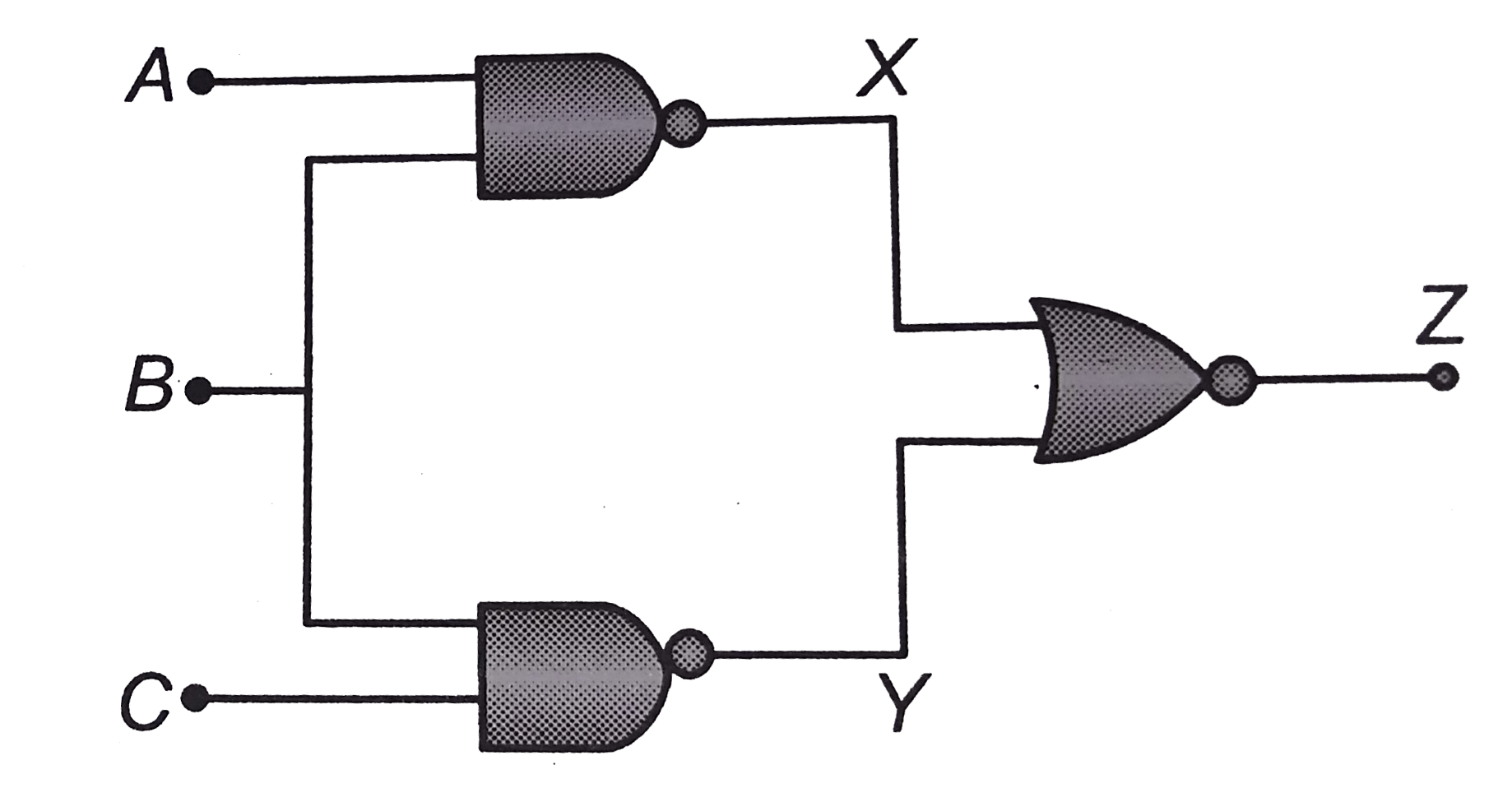
View SolutionThe diagram of a logic circuit is given below. The output `F` of the circuit is represented by
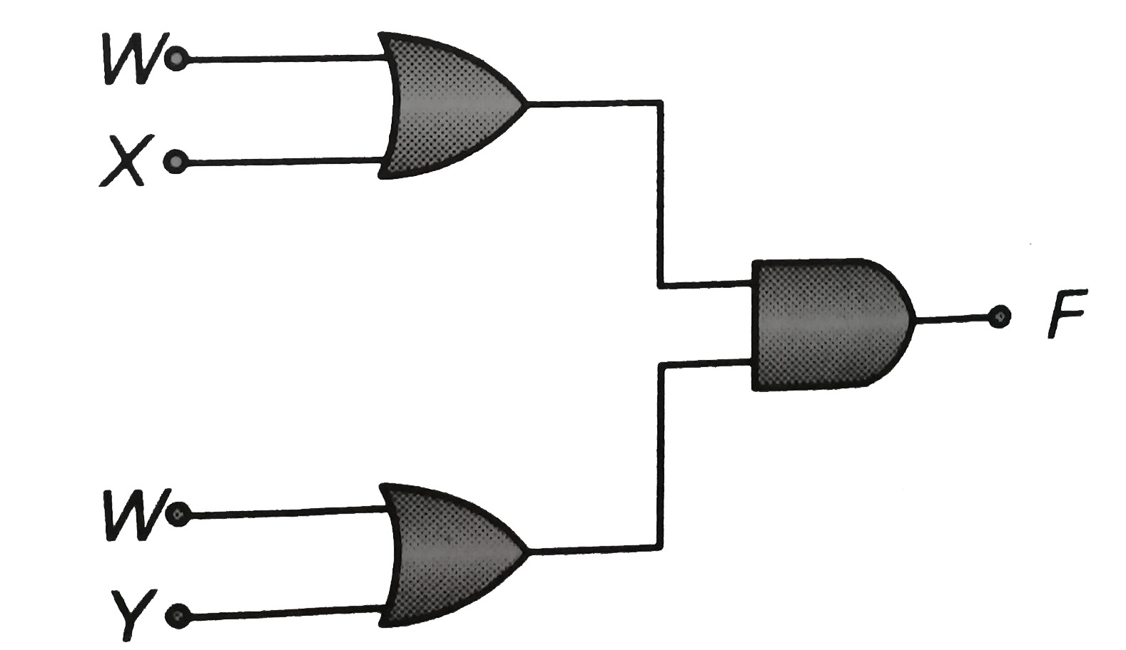
View SolutionIn circuit in the following figure the value of `Y` is

View Solution
Digital Electronics questions and complete solutions for chapter SEMICONDUCTOR ELECTRONICS of A2Z PHYSICS (HINGLISH) of Class 12