Complete Solutions to Problems Based On Mixed Concepts of chapter SEMICONDUCTOR ELECTRONICS of Class 12 book with complete answers and questions
| Class 12 | PHYSICS |
| Chapter | SEMICONDUCTOR ELECTRONICS |
| A2Z | Problems Based On Mixed Concepts |
| Number Of Questions | 32 |
| Academic Year | 2023-24 |
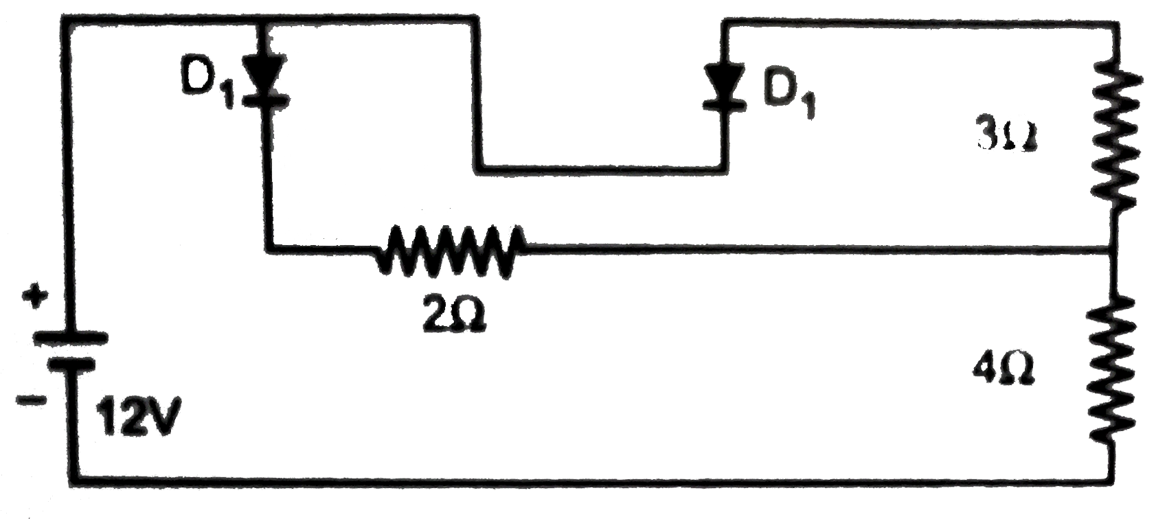
In the circuit of figure. Treat the diodes as ideal. Current in the `4` ohm resistor is
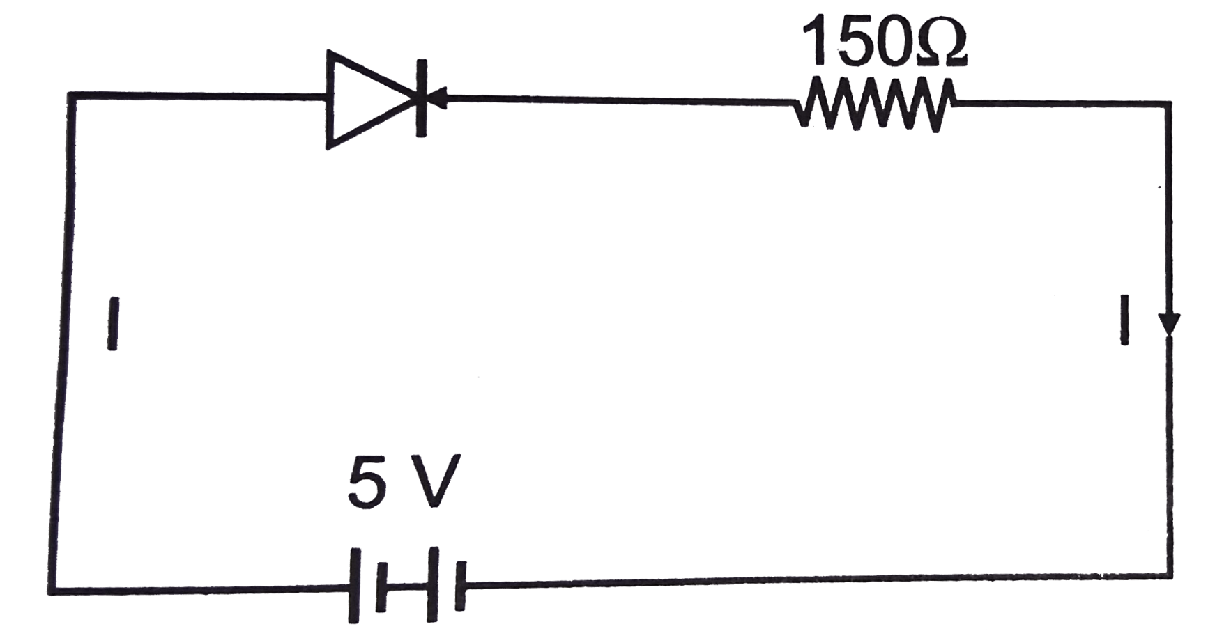
View SolutionThe potential barrier developed in the diode of figure is `0.5 V`. The current in the diode is current in the diode is
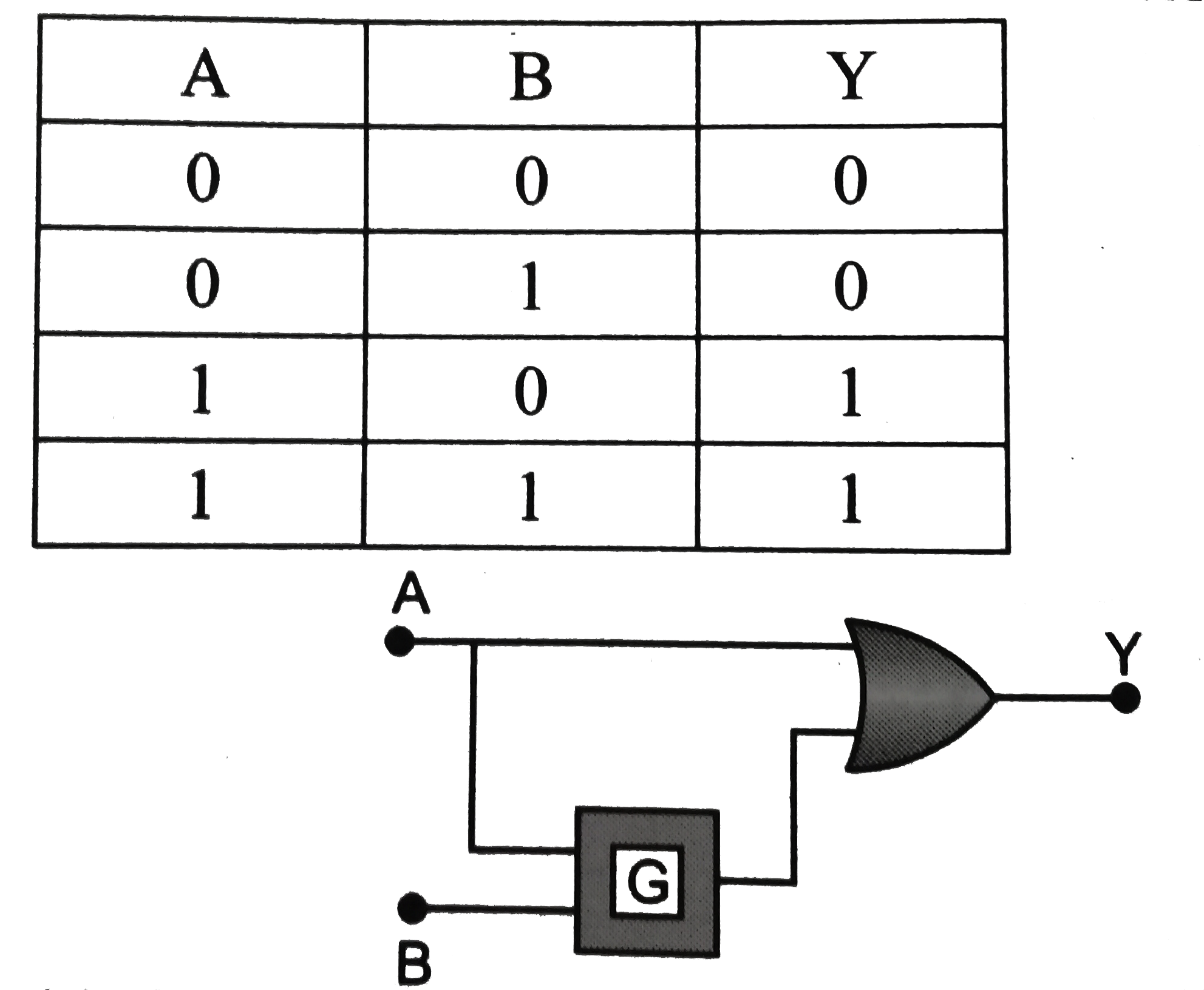
View SolutionIdentify the logic gate `G` in the combination of gates shown in fig. The truth table is shown here
View SolutionThe current amplification of the common base `NPN` transistor is `0.96`. What is the current gain if it is used as common emitter amplifier?
View SolutionIn figure the current supplied by the battery is

View SolutionFigure shows a piece of semiconductor (pure one) `S` in series with a variable resistor `R` and a source of constant voltage `V. S` is heated and the current is kept constant by adjustment `R`. Which of the following factors will decrease during this process?
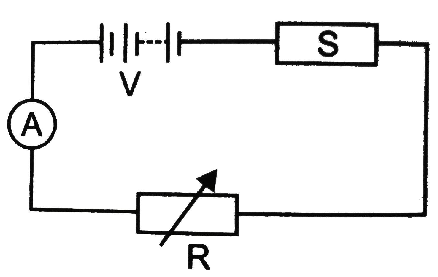
`(1)` The drift velocity of the conduction electrons in `S`.
`(2)` The `DC` resistance of `S`
`(3)` The number of conduction electrons in `S`. which of the following is correct?
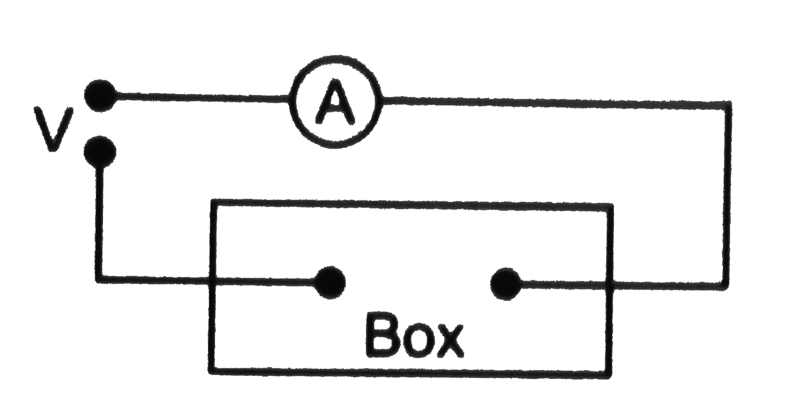
View SolutionA semiconductor diode and a resistor of constant resistance are connected in some way inside a box having two external terminals. When a potential difference `V` of `1V` is applied, `1=25 mA`. If potential difference is reversed, `I=50 mA`. Forward resistance and diode resistance are
View SolutionA transistor is used in a common-emitter mode in an amplifier circuit. When a single of `20 mV` is added to the base-emitter voltage, the base current change by `20 muA` and the collector current changes by `2mA`. The load resistor in `5kOmega`. What is the volume of `beta`?
View SolutionA transistor is used in common-emitter mode in an amplifier circuit. When a signal 20mV is added to the base-emmiter voltage,the base current changes by `20(mu)A `and the collector current changes by 2mA.The load resistance is `5k(Omega)`.Calculate (a)the factor`(beta)`(b)the input resistance `R_(BE),`(c) the transconductance and (d) the voltage gain .
View SolutionA transistor is used in common-emitter mode in an amplifier circuit. When a signal 20mV is added to the base-emmiter voltage,the base current changes by `20(mu)A `and the collector current changes by 2mA.The load resistance is `5k(Omega)`.Calculate (a)the factor`(beta)`(b)the input resistance `R_(BE),`(c) the transconductance and (d) the voltage gain .
View SolutionIn a common emitter amplifier, using output reisistance of `5000` ohm and input resistance fo `2000`ohm, if the peak value of input signal voltage is `10 m V` and `beta=50`, then the peak value of output voltage is
View SolutionIn a common emitter amplifier, using output reisistance of `5000` ohm and input resistance fo `2000`ohm, if the peak value of input signal voltage is `10 m V` and `beta=50`. The power gain is
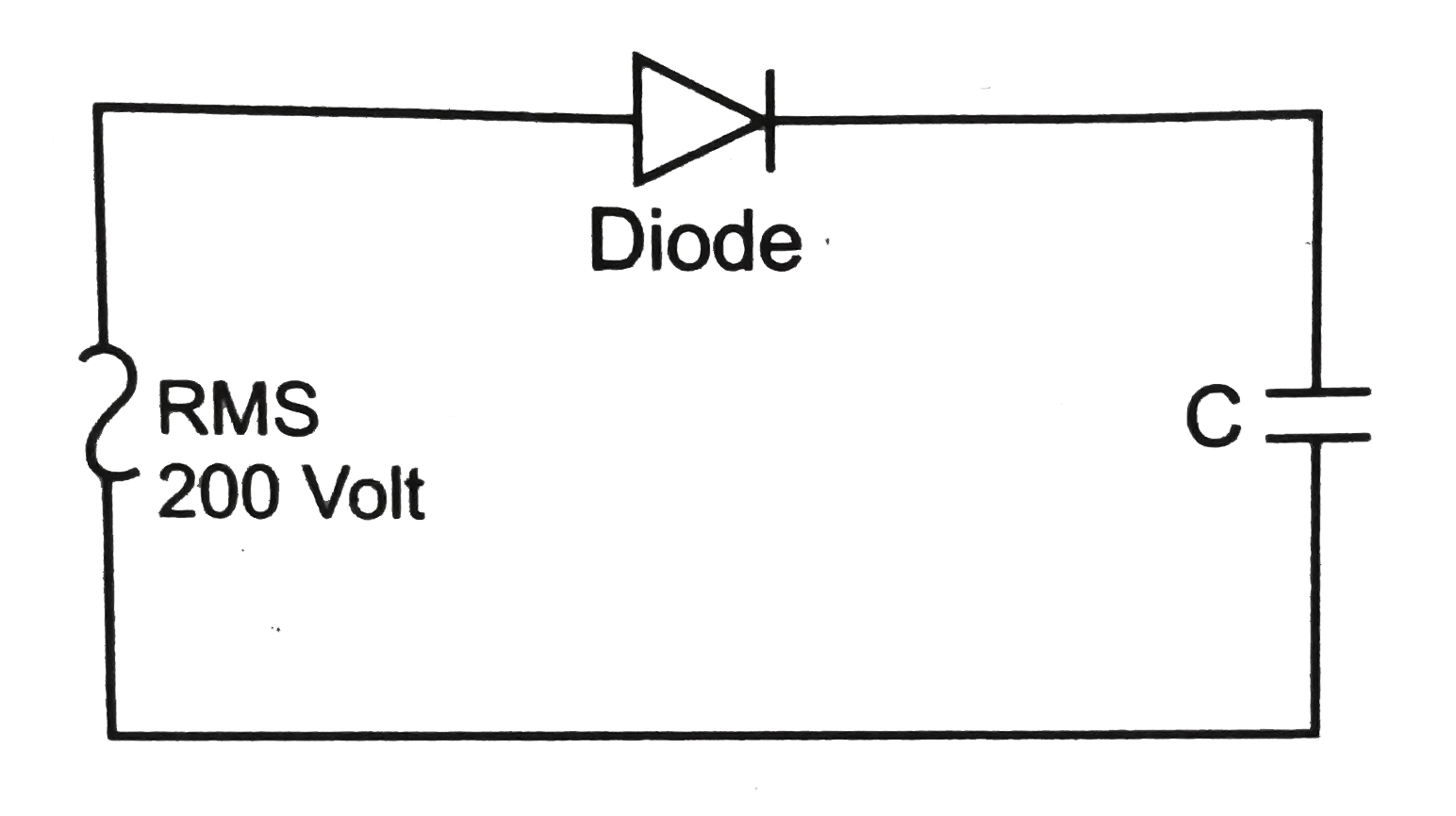
View SolutionA sinusiodal voltage of `rms` value `200` volt is connected to the diode and capacitor `C` in the shown so that half wave reactification occurs. The final potential difference in volt across `C` is
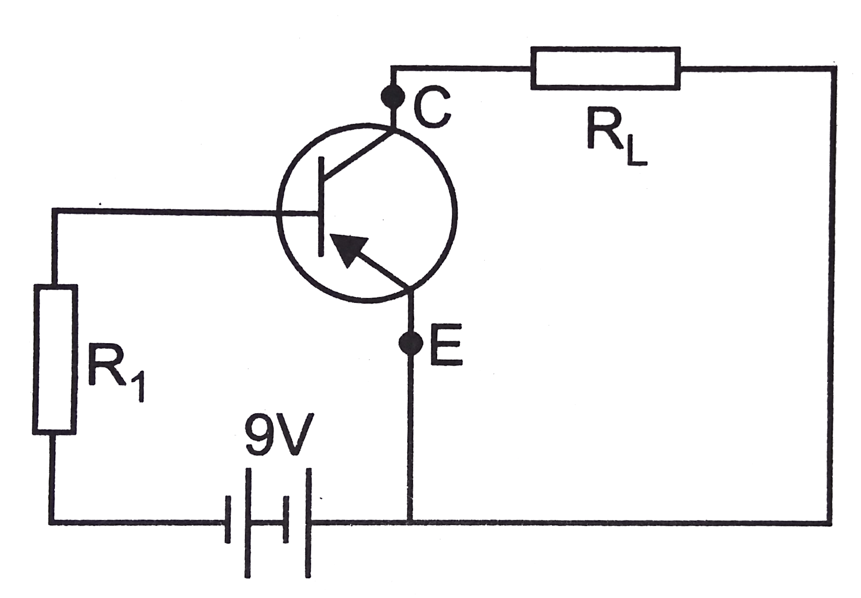
View SolutionIn the circuit shown, the base current is `30muA`. The value of `R_(1)` is
View SolutionThe diagram shows a logic network.
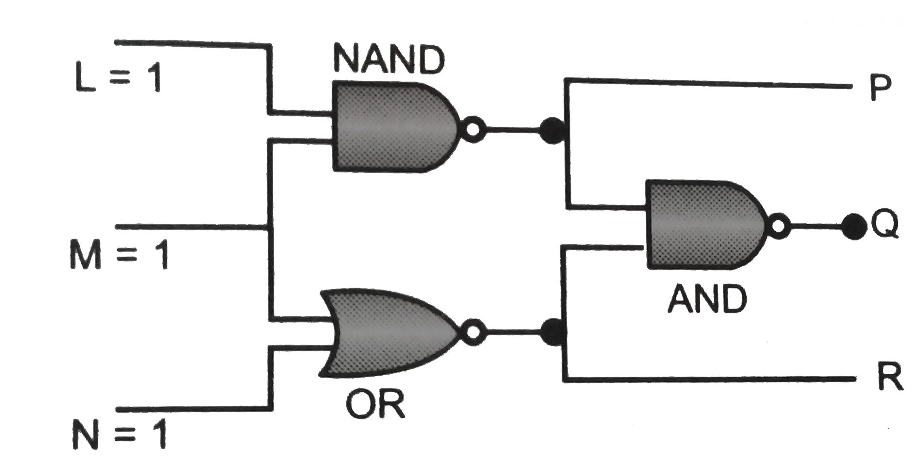
If the inputs `L,M` and `N` are all at logic `1`, what are the logic states of `P,Q` and `R`?
View SolutionIn the circuit shown in the diagram, the operational amplifier may be assumed to be ideal. The current in the `12 kOmega` resistor is `I`.
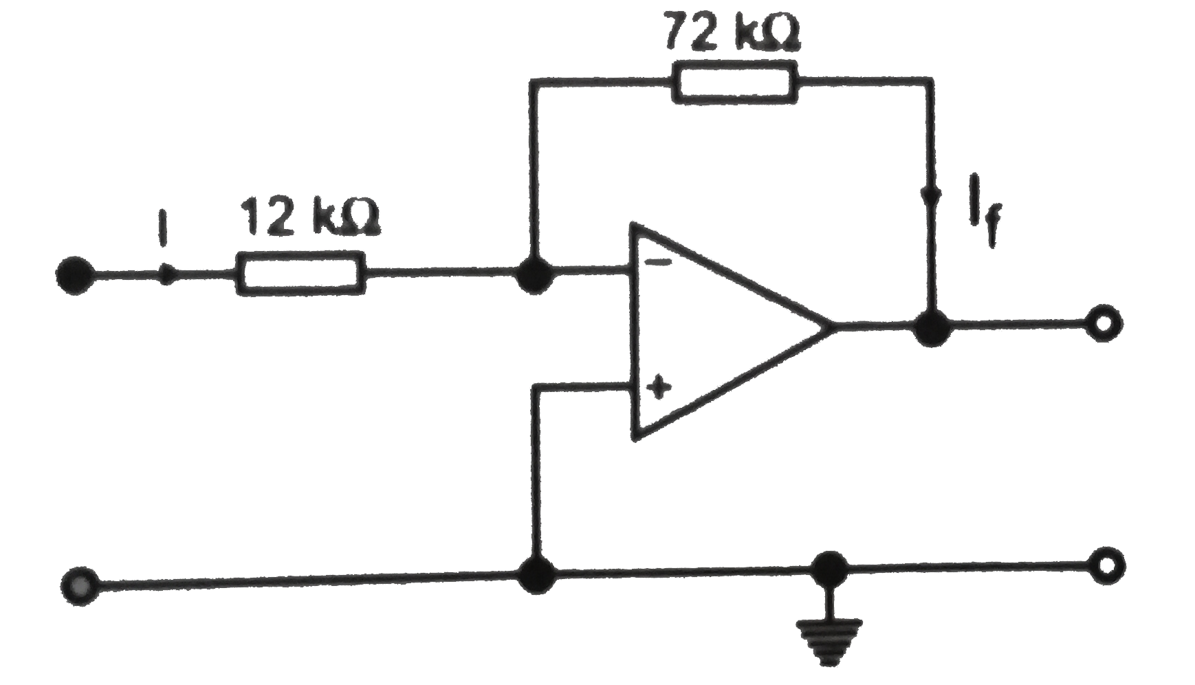
What is the current `I_(f)` in the `72 k Omega` resistor?
View SolutionAn input voltage `V_(i)` of `0.20 V` is applied to an operational amplifier connected as shown in the diagram. What is the output voltage `V_(0)`?
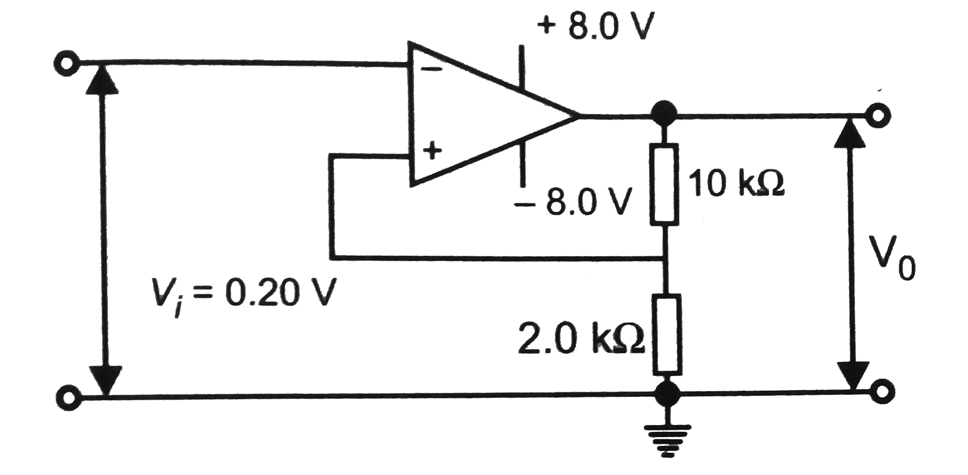
View SolutionThe function of a half -adder may be represented as shown in Figure.

A full-adder may be constructed from two half-adders together with a single logic gate as shown in figure.

Which logic gate must be used?
View SolutionThe diagram shows an operational circuit. Which of the following correctely states the nature and magnitude of the amplification ?
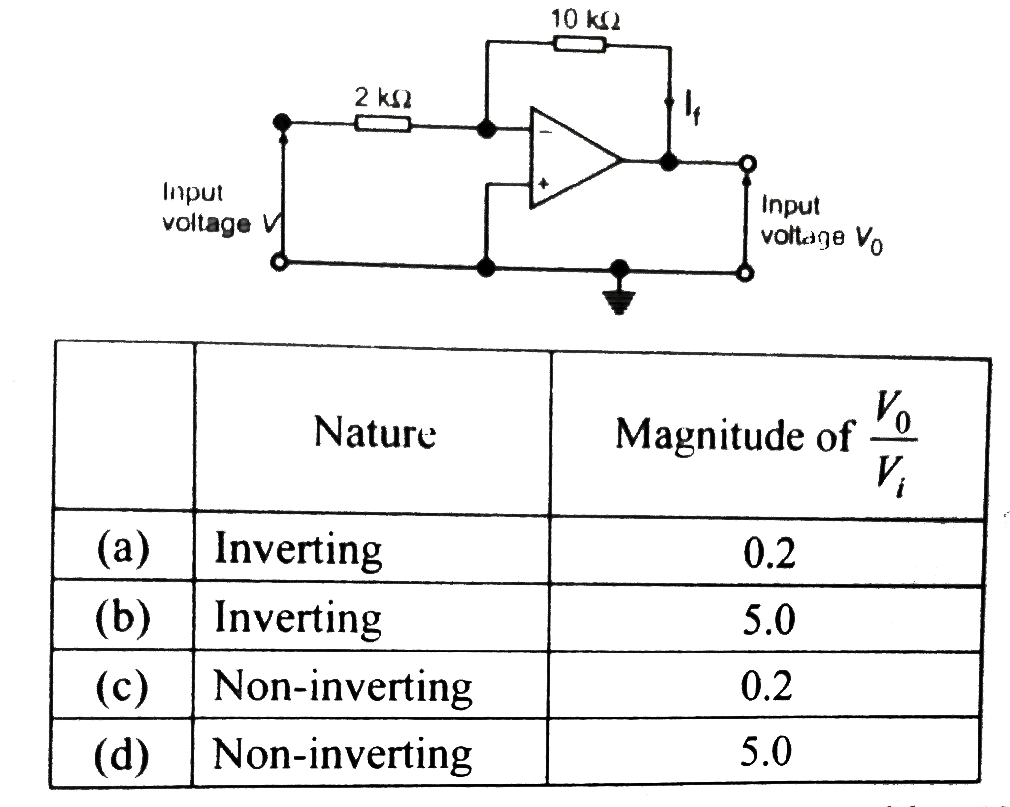
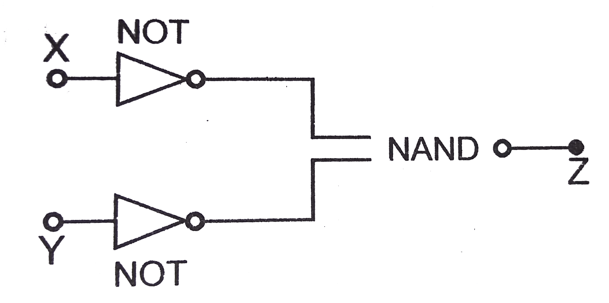
View SolutionA digital system comprises a `HAND` gate with a `NOT` gate on each of its inputs as shown in figure.
To which of the following single gate is this system equivalent?
View SolutionA combination of logic gates has the truth table below
`|(P,Q,Z),(0,0,0),(0,1,1),(1,0,1),(1,1,1)|`
Which combination has this table?
View SolutionIdentify the gate in figure.
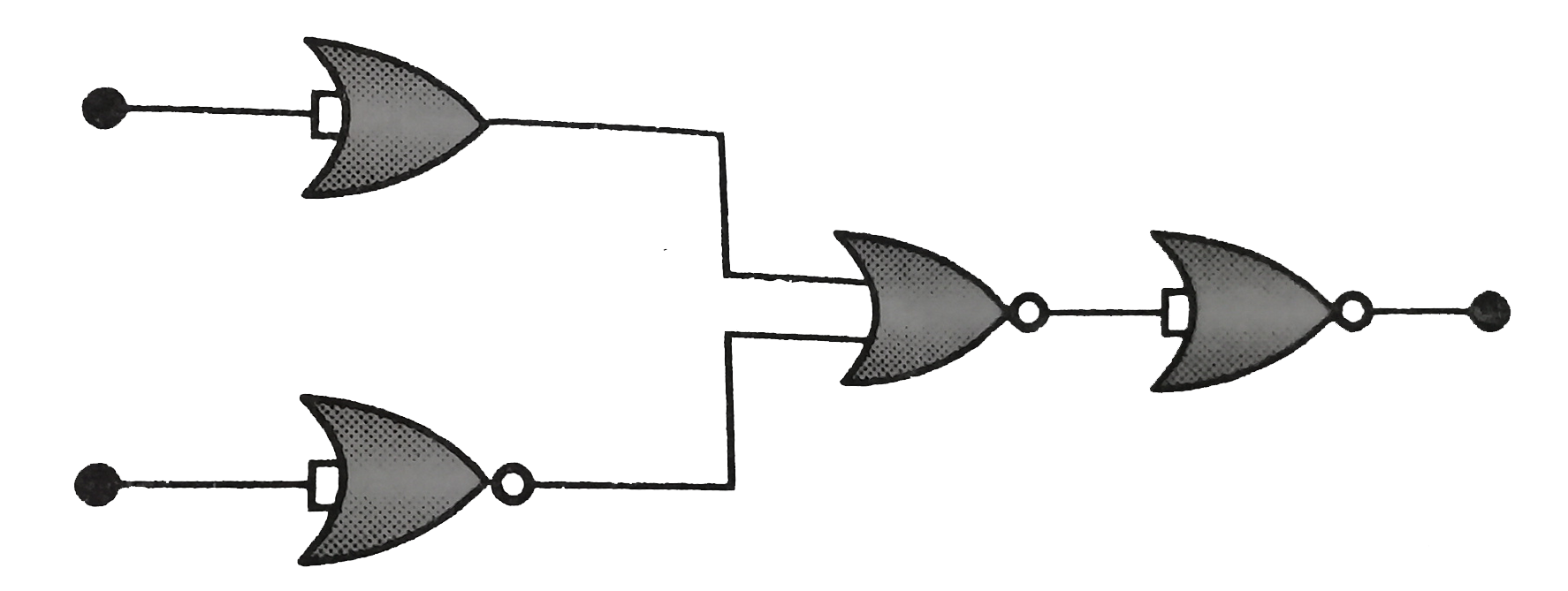
View SolutionWhat is the output in the given figure?

View SolutionThe diagram shows a logic network.
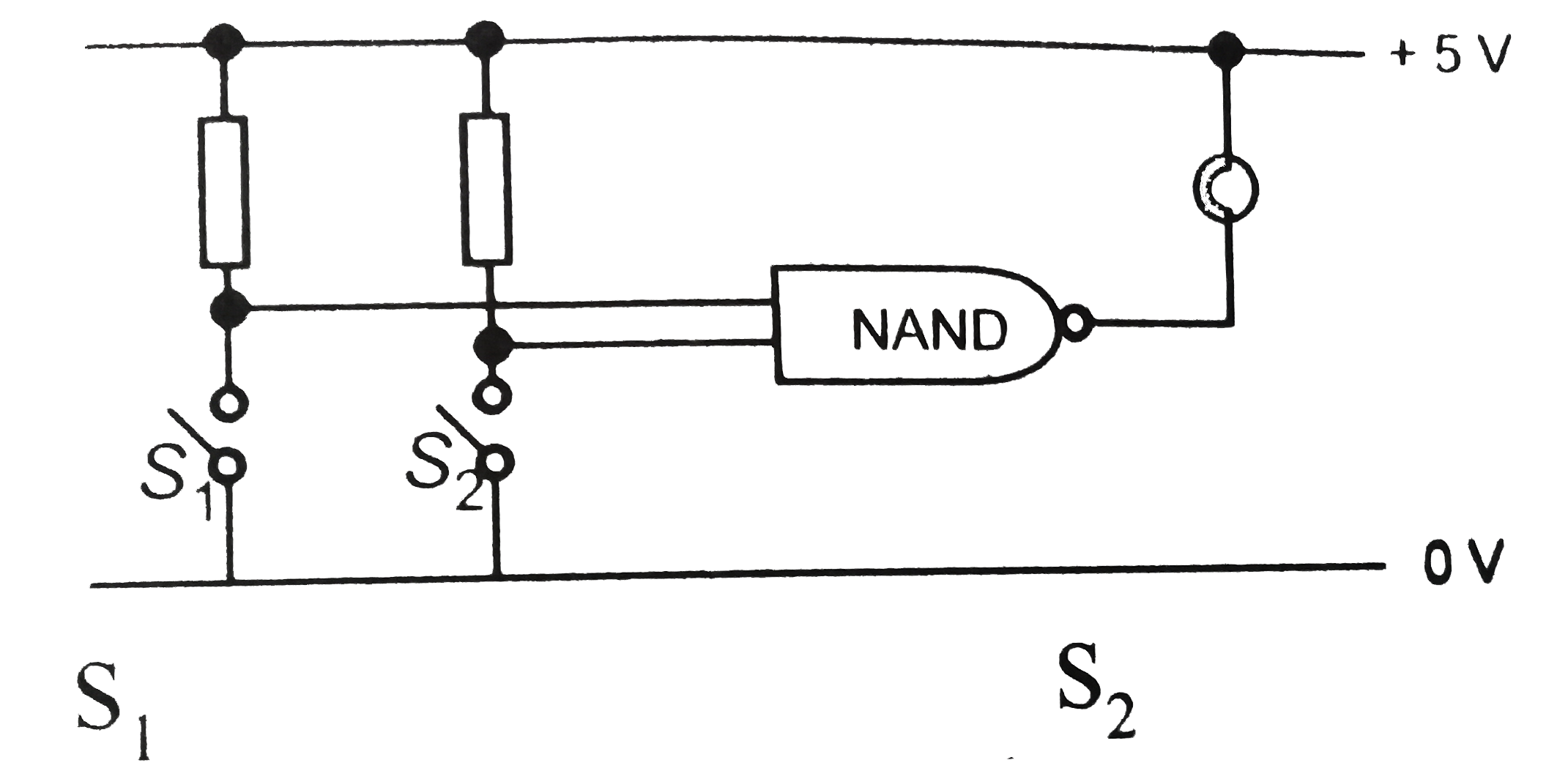
Which single gate is equivalent to the network?
View SolutionFor the given combination of gates, if the logic states of inputs `A,B,C,` are as follows `A=B=C=0` and `A=B=1, C=0` then the logic states of output `D` are
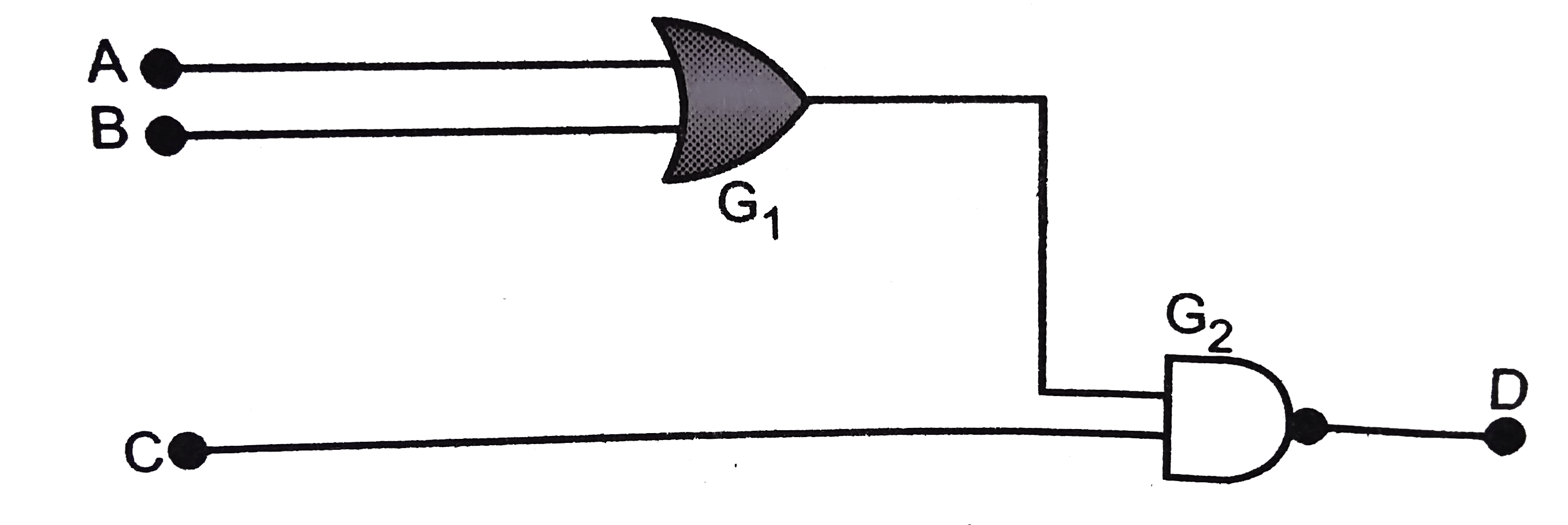
View SolutionFigure shows a combination of logic gates. To what single gate is this combination equivalent?

View SolutionLogic gates `X` and `Y` have the truth tables shown below

`|(P,Q,R,P,R),(0,0,0,0,1),(1,0,0,1,0),(0,1,0,,),(1,1,1,,)|`
When the output of `X` of connected to the input of `Y`, the resulting combination is equivalent to a single.
View SolutionFigure shows a circuit designed to control a lamp. For what positions of the switches `S_(1)` and `S_(2)` will the lamp the lit?
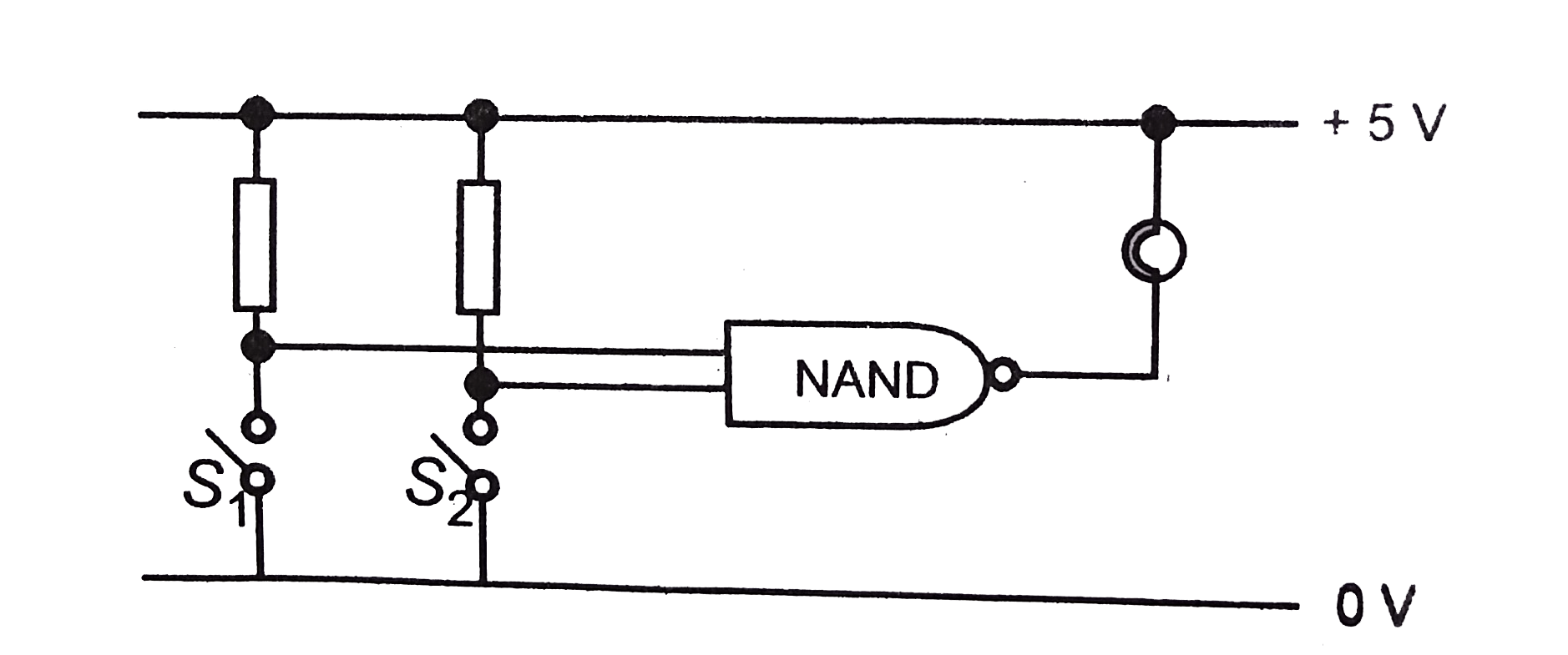
View SolutionThe typical ionisation energy of a donor in silicon is
View SolutionIn `PN`-junction diode the reverse saturation curren is `10^(-5)` amp at `27^(@)C`. The forward current for a voltage of `0.2` volt is
View SolutionA potential difference of `2V` is applied between the opposite faces of a `Ge` crystal plate of area `1 cm^(2)` and thickness `0.5 mm`. If the concentration of electrons in `Ge` is `2xx10^(19)//m^(3)` and mobilities of electrons and holes are `0.36(m^(2))/(vol t-sec)` and `0.14 (m^(2))/(vol t-sec)` respectively, then the current flowing through the plate will be
View SolutionThe contribution in the total current flowing through a semiconductor due to electrons and holes are `3/4` and `1/4` respectively. If the drift velocity of electrons is `5/2` times that of holes at this temperature, then the ratio of concentration of electrons and holes is
View Solution
Problems Based On Mixed Concepts questions and complete solutions for chapter SEMICONDUCTOR ELECTRONICS of A2Z PHYSICS (HINGLISH) of Class 12