Exercise from PRADEEP PHYSICS Chapter 7 ELECTRONIC DEVICES for Class 12
| Class 12 | PHYSICS |
| Chapter | ELECTRONIC DEVICES |
| PRADEEP PHYSICS | Exercise |
| Medium | English |
| Academic Year | 2023-2024 |
Question 39
Draw the "energy bands" diagram for a (i) pure semiconductor (ii) insulator. How does the energy band, foe a pure semiconductor, get affected when this semiconductor is doped with an acceptor impurity donor impurity? Hence discuss why the 'holes' and the 'electrons' respectively, become the 'majority charge carriers' in these two cases.View SolutionQuestion 50
A semiconductor has equal electron and hole concentration of 6×10⁸/m3. On doping with certain impurity, electron concentration increases to 9×10¹²/m3. (i) Identify the new semiconductor obtained after doping. (ii) Calculate the new hole concentration. (iii) How does the energy gap vary with doping?View SolutionQuestion 57
Determine the number density of donor atoms which have to be added to an intrinsic germanium semiconductor to produce an n-type semiconductor of conductivity 5Ω−1cm−1, given that the mobility of electron in n-type germanium is 3900cm2V−1s−1. Neglect the contribution of holes to conductivity.View SolutionQuestion 61
Find the current produced at room temperature in a pure germanium plate of area 2×10⁻⁴m2 and of thickness 1.2×10⁻³m when a potential of 5V is applied across the faces. Concentration of carries in germanium at room temperature is 1.6×10⁶ per cubic metre. The mobilities of electrons and holes are 0.4m2V−1s−1 and 0.2m2V−1s−1 respectively. The heat energy generated in the plate in 100 second is.View SolutionQuestion 62
If resistivity of pure silicon is 3000Ωmeter, and the electron and hole mobilities are 0.12m2V−1s−1 and 0.045m2V−1s−1 respectively, determine the resistivity of a specimen of the material when 1019 atoms of phosphorous are added per m3 are also added. Given charge on electron =1.6x10⁻¹⁹C.View SolutionQuestion 65
The width of depletion region in a P-N junction diode is 500 nm and an intense electric field of 5×10⁵Vm−1 is also found to exit init. Determine the height of the potential barrier. Also calculate the kinetic energy which a conduction electron must have inorder to diffuse from the n-side to p-side.View SolutionQuestion 67
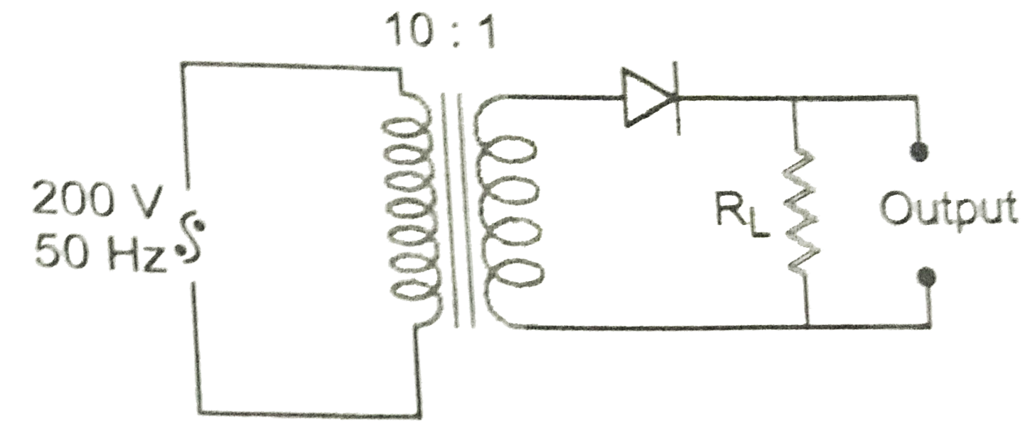
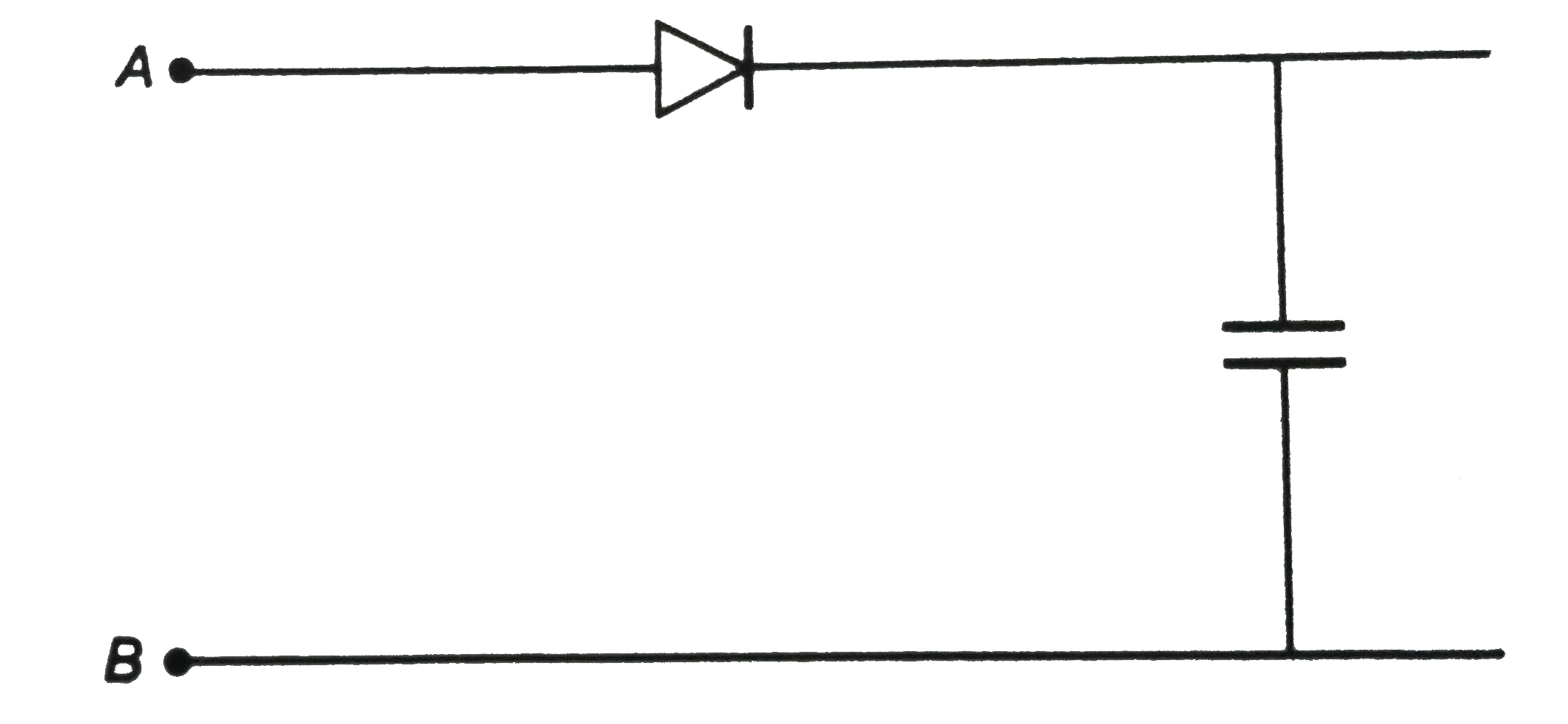
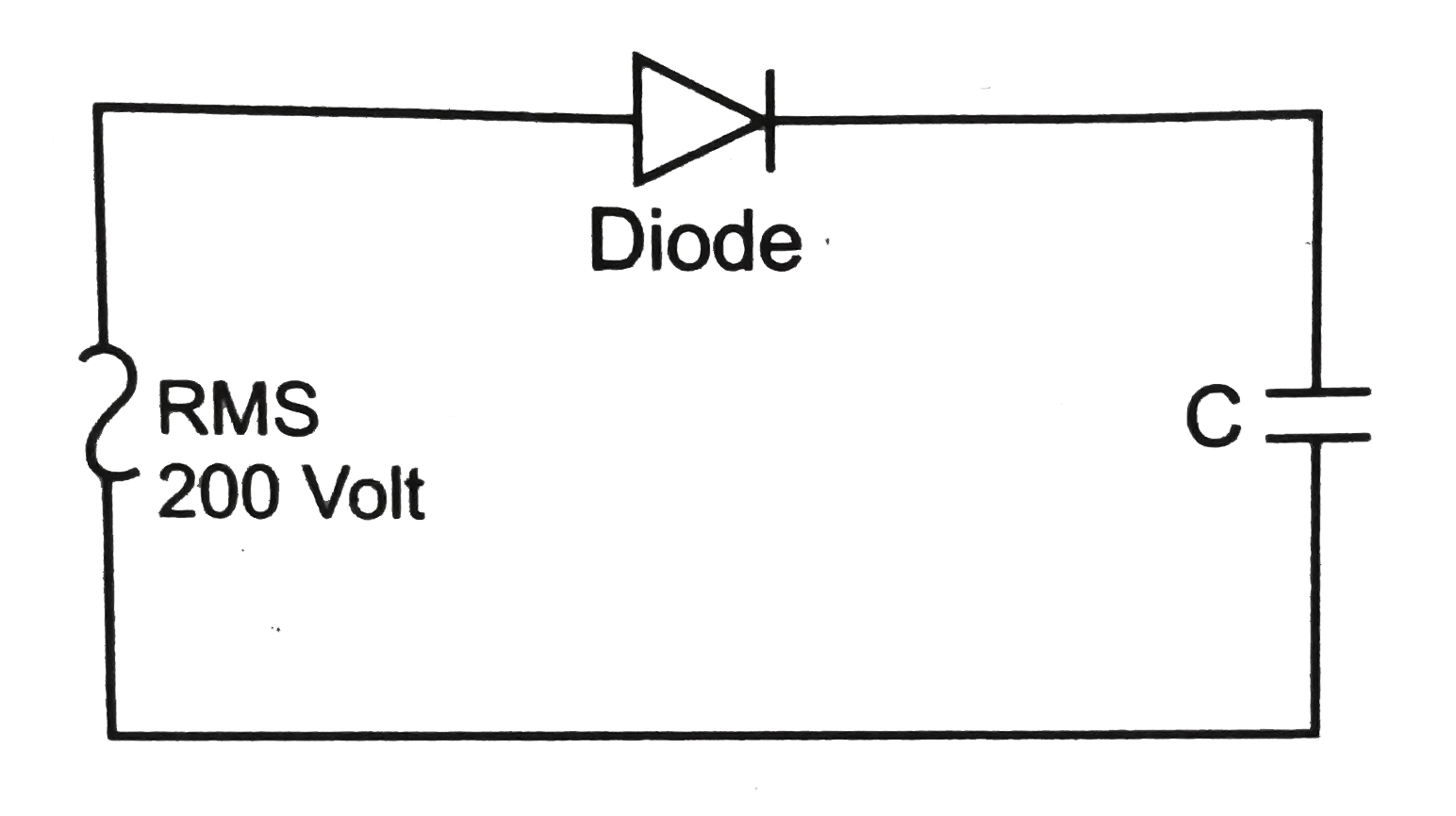
A sinusoidal voltage of rms value 200 volt is connected to a diode and a resistor R in the circuit as shown in Fig., so that half wave rectification occurs. If the diode is ideal, what is the rms voltage across R? If resistor R is replaced by capactior of capacitance C, find the potential difference across C.
 View Solution
Question 69
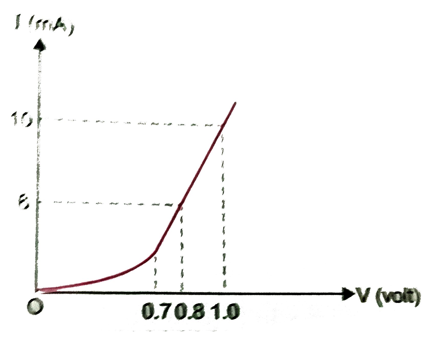
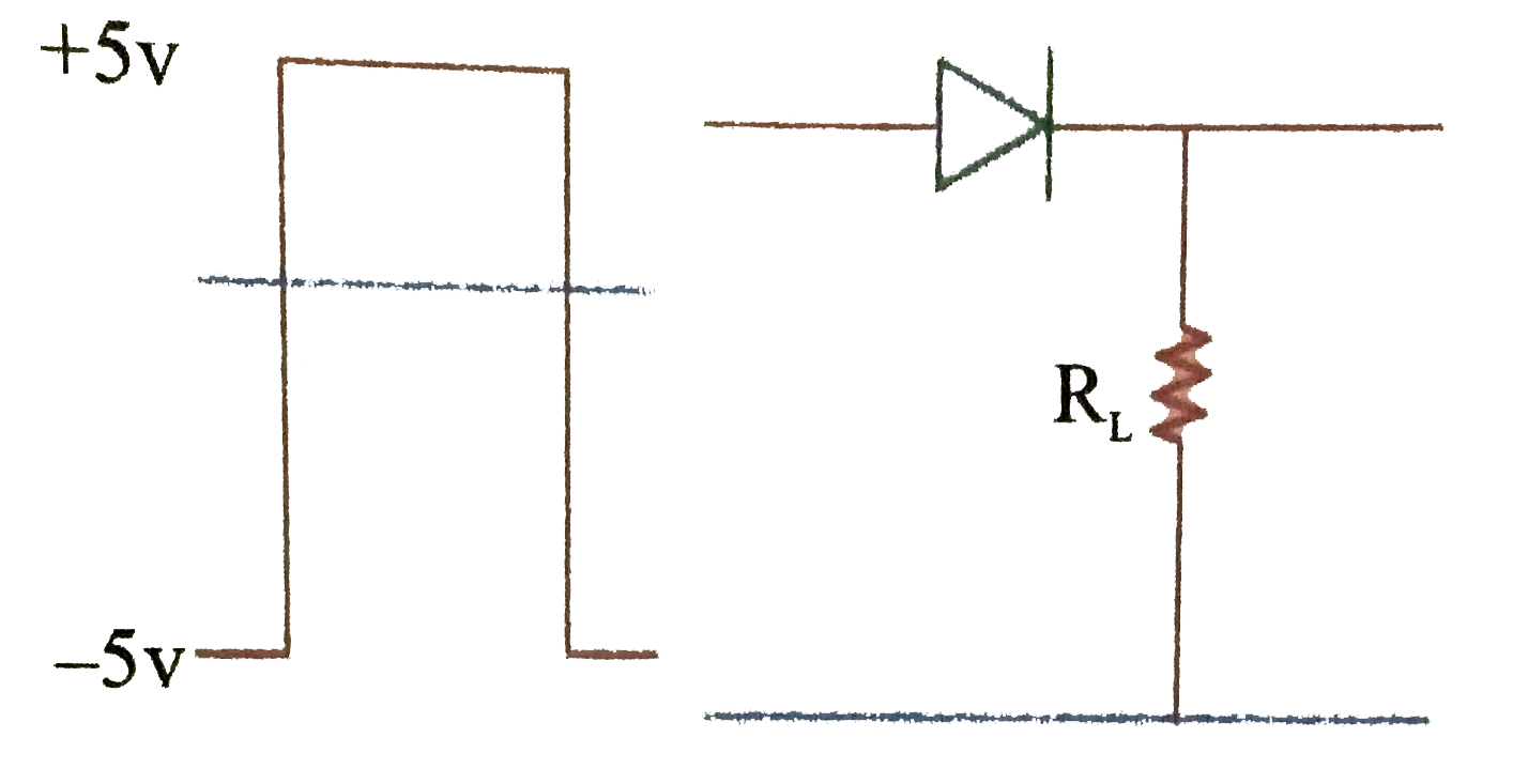
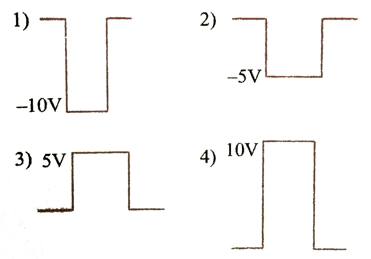
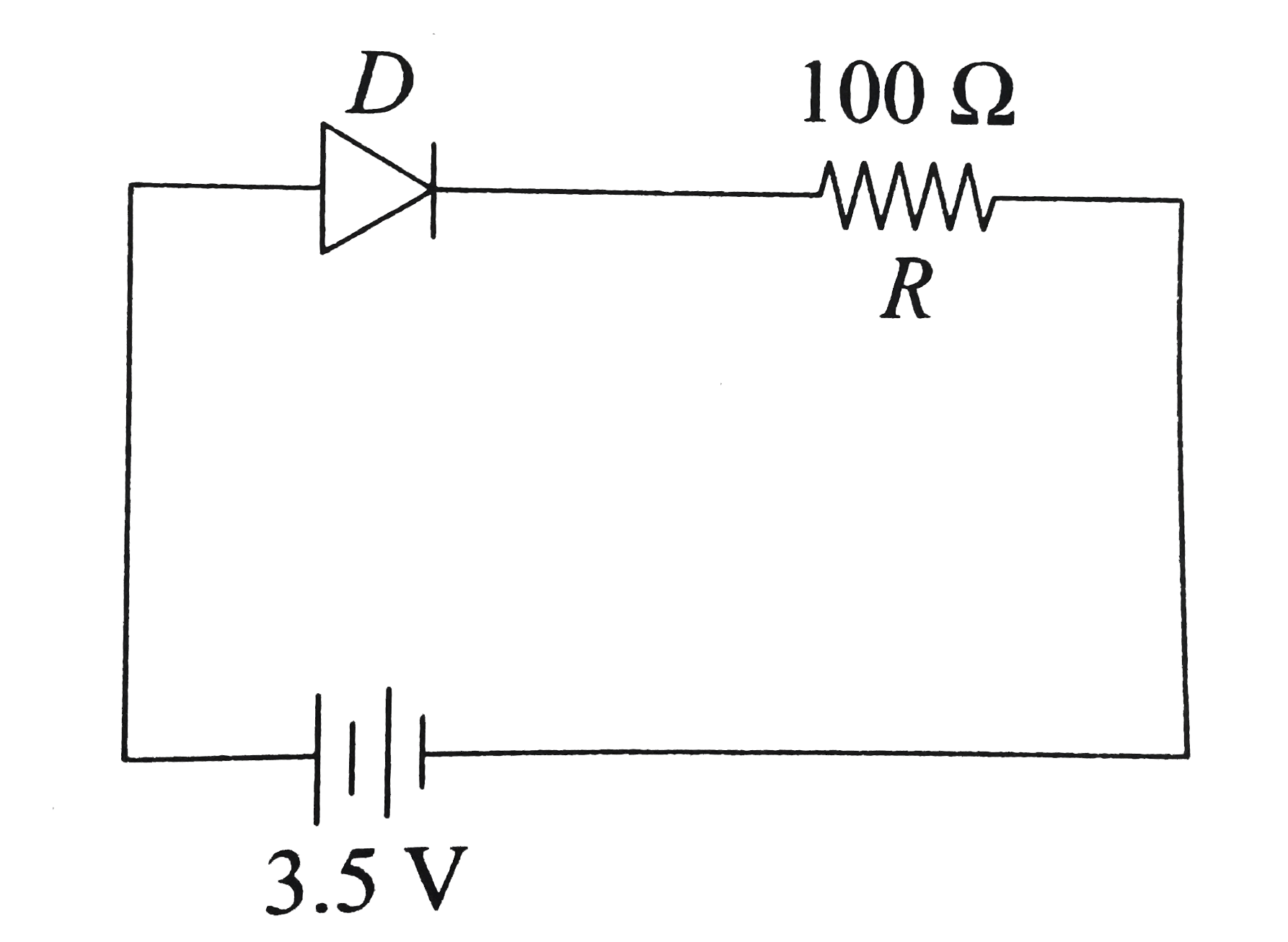
A silicon p-n junction diode whose knee voltage is 0.7V is connected to a battery with supply voltage 3V and 100mA in forward biasing. If a resistor R is used in series of the circuit, then a current of 20mA passes through the diode. Find the wattage of the resistor and of the diode.View SolutionQuestion 79
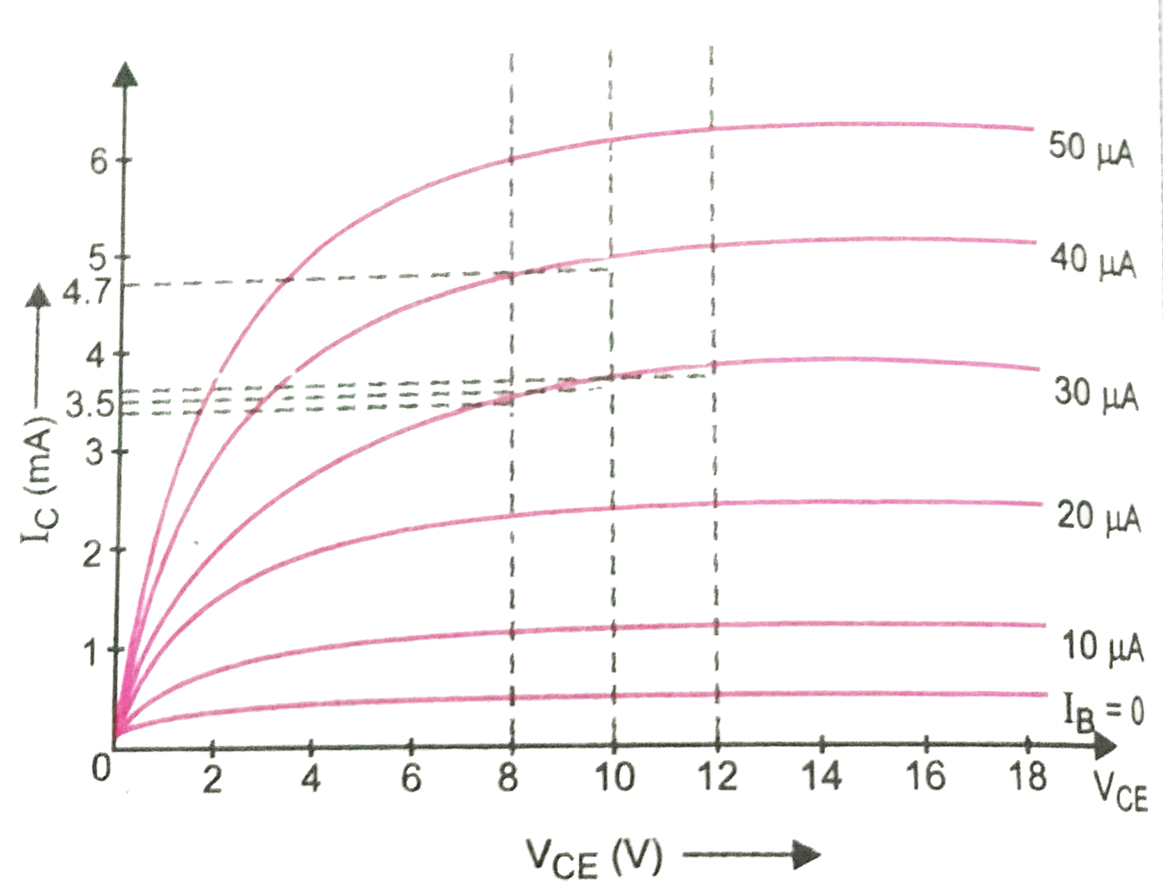
In a silicon transistor, base current is changed by 20μA. This result in a change of 0.02V in base-emitter voltage and a change of 2mA in the collector current.
Find the input resistance, βa.c. and transconductance of the transistor.
The transistor is used as an amplifier with the load resistance 5kΩ. What is the voltage gain of the amplifier?View SolutionQuestion 80
The input resistance of a silicon transistor is 665Ω. Its base current is changed by 15μA which result in the change in collector current by 2mA. This transistor is used as a common emitter amplifier with a load resistance of 5kOmega calculate current gain, βa.c., transconductance gm and voltage gain Av of the amplifier.View SolutionQuestion 82
A change of 0.2mA in the base current cause a change of 5mA in the collector current for a common emitter amplifier. (i) Find the a.c. current gain of the transistor (ii) If the input resistance is 2kΩ and its voltage gain is 75. Calculate the load resistance used in the circuit.View SolutionQuestion 83
A transistor is used in common-emitter mode in an amplifier circuit. It is found that when a signal of 20mV is added to the base-emitter voltage, the base current changes by 20μA and collector current changes by 1.5mA. Determine the factor beta, input resistance Ri, the transconductance and voltage gain, Given load resistance RL=6kΩ.View SolutionQuestion 84
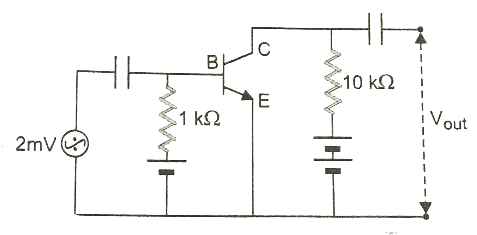
For a common emitter transistor amplifier, the audio signal voltage across the collector resistance of 2kΩ is 2V. If the current amplification factor of the transistor is 100, calculate (i) input signal voltage (ii) base current and (iii) power gain. Given that the value of the base resistance is 1kΩ.View SolutionQuestion 85
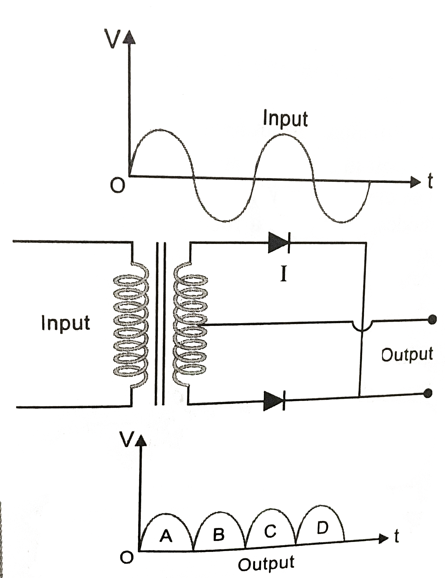
A full wave rectifier uses two diodes, the internal resistance of each diode may be assumed constant at 30Ω. The transformer r.m.s. secondary voltage from centre tap to each end of the secondary is 50 V and load resistance is 970Ω. Find (i) the mean load current (ii) the rms value of load current.View SolutionQuestion 88
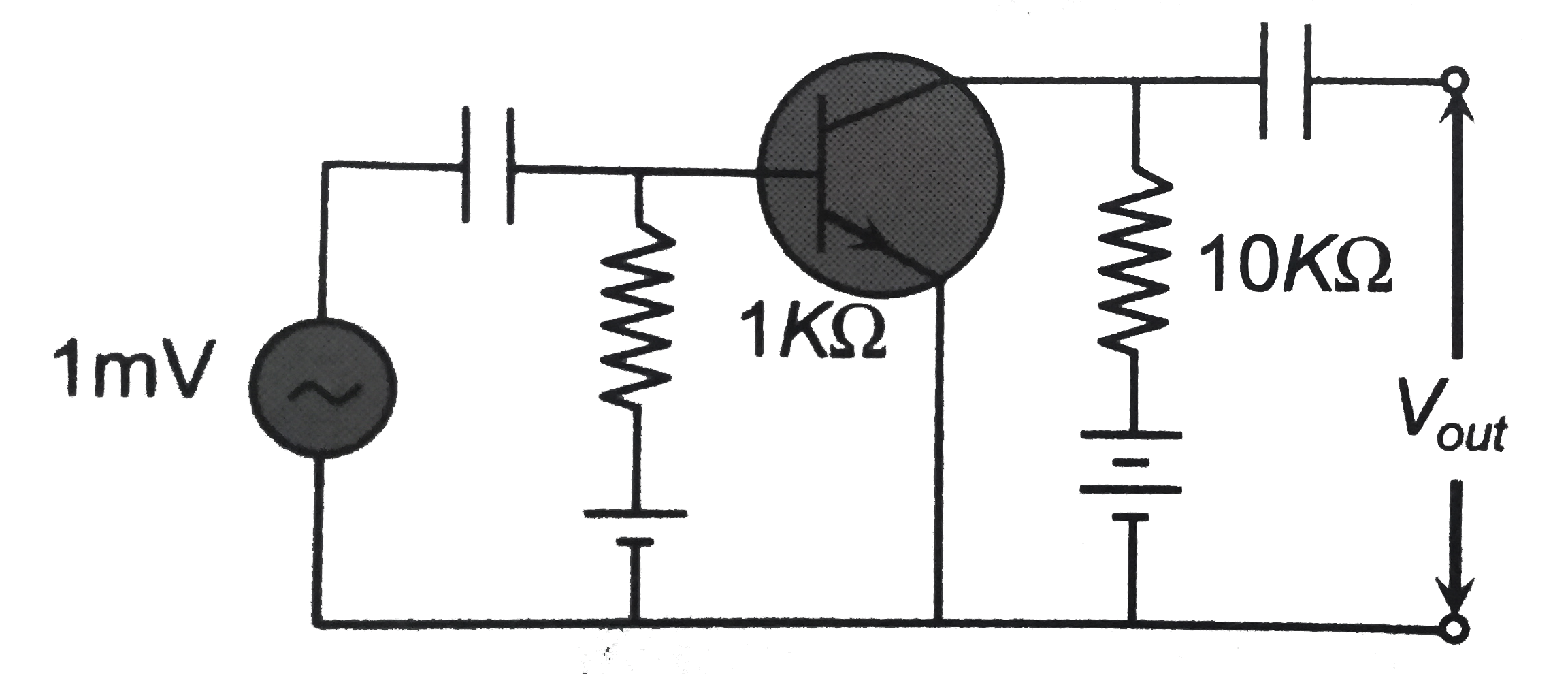
In a common emitter transistor amplifier, the input resistance of a transistor is 1000Ω. On changing its base current by 10muA, the collector current increases by 2mA. If a load resistance of 5kΩ is used in the circuit, calculate:
(i) the currnet gain (ii)the voltage gain of the amplifier.View SolutionQuestion 91
In a centre trap full wave rectifier, the load resistance RL=1kΩ. Each diode has a forward bias dynamic resistance 20Ω. The voltage across half the secondary winding is 110 sin 100 pit. Find (i) the peak value of current (ii) the dc value of current (iii) the rms value of current.View SolutionQuestion 108
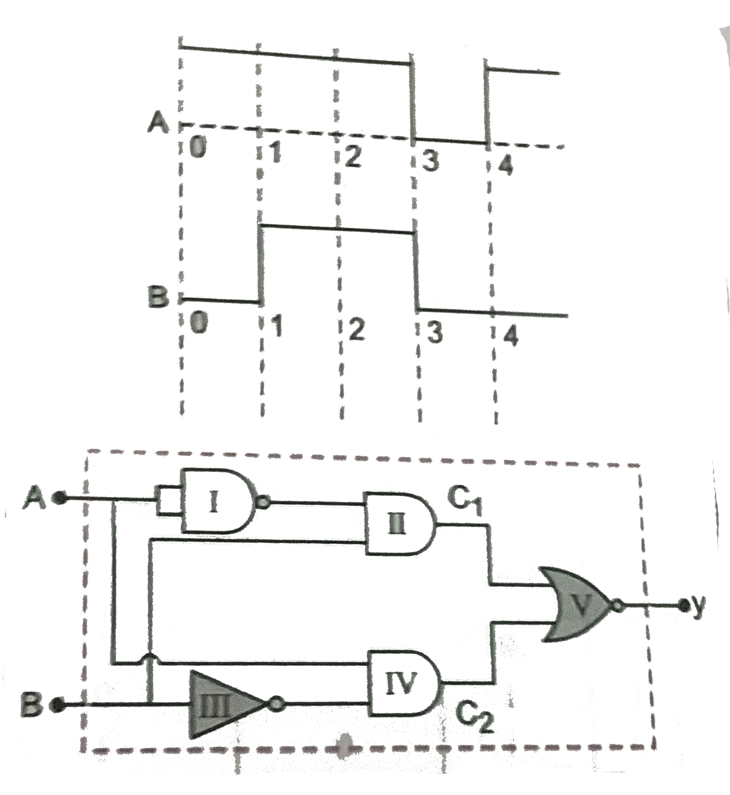
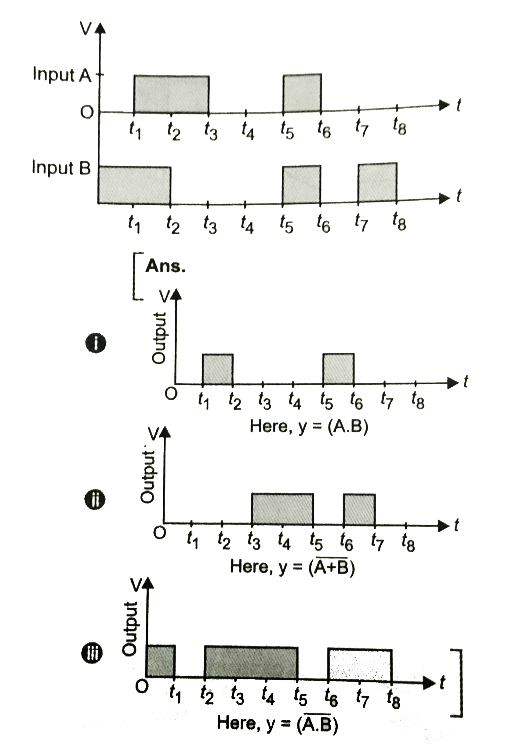
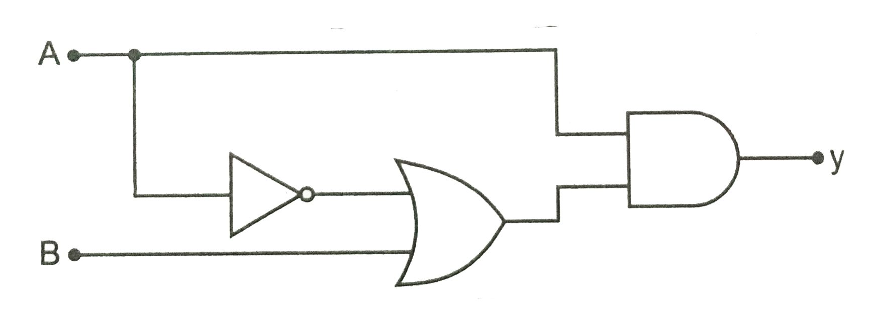
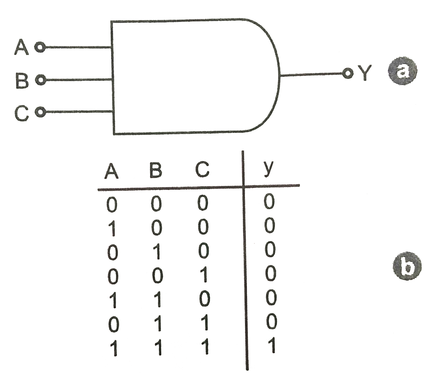
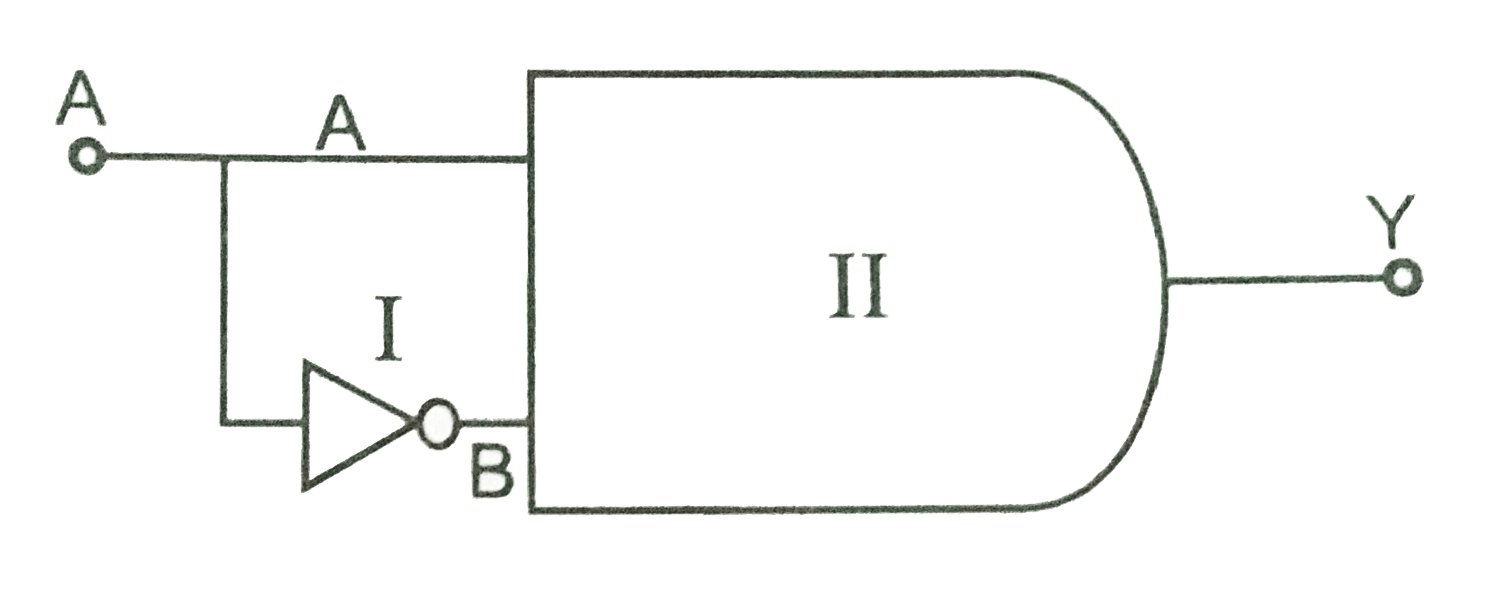
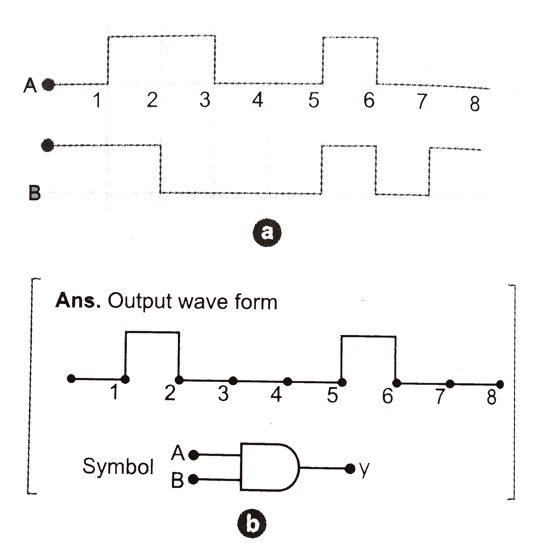
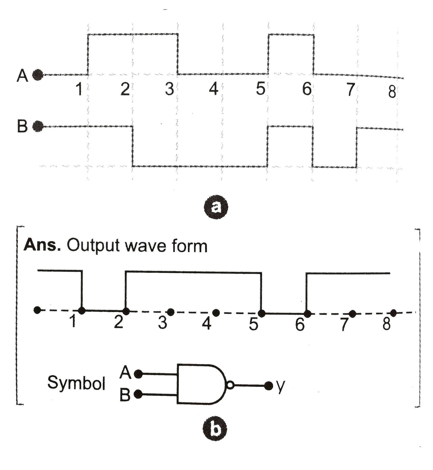
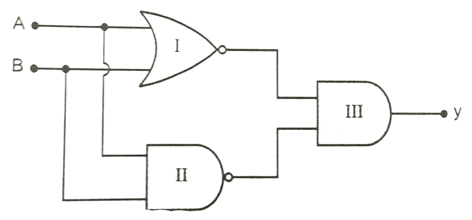
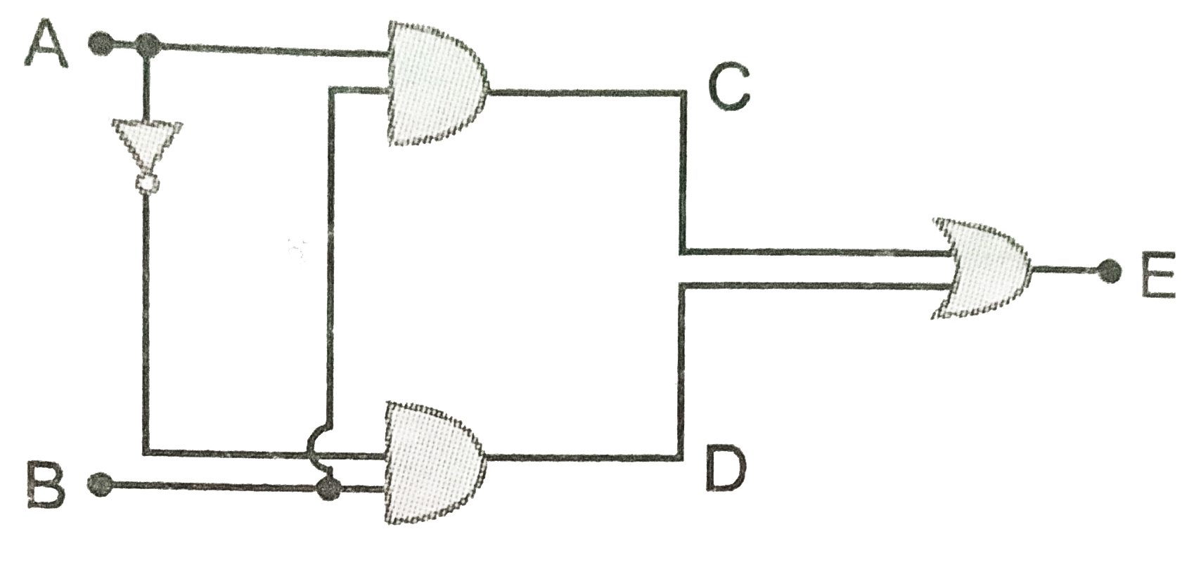
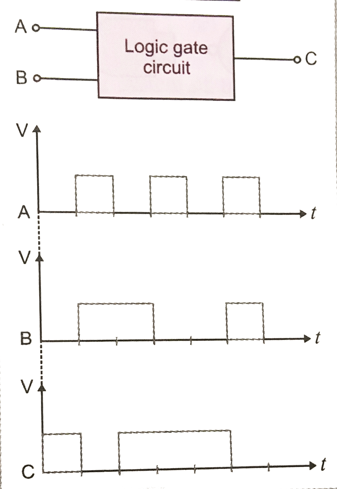
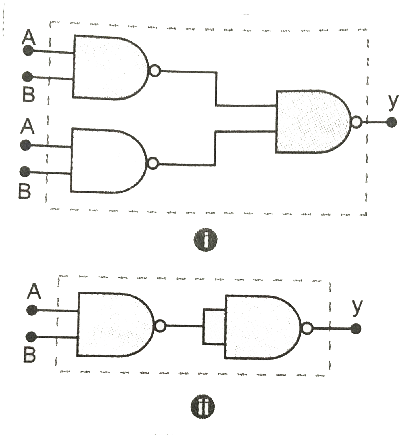
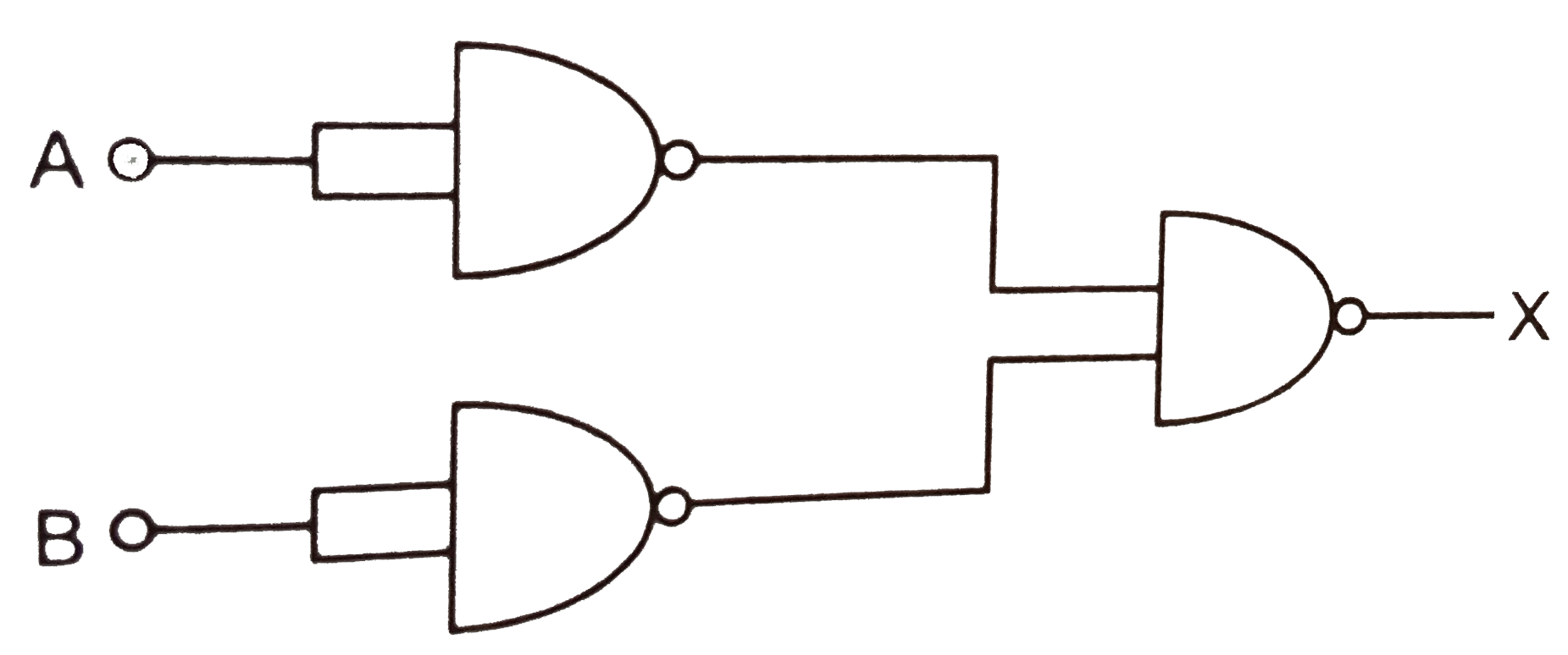
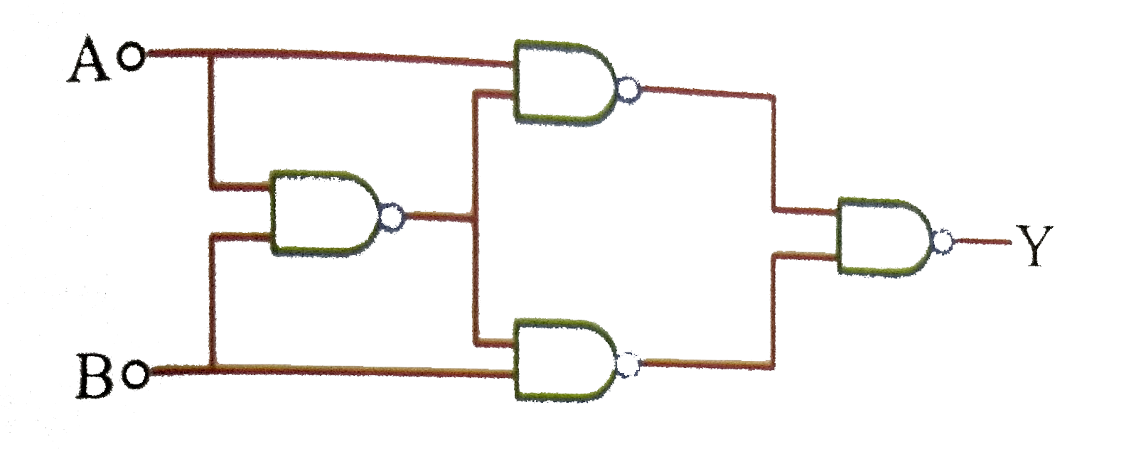
Input signal A and B are applied to the input terminals of the 'dotted box' set up shown here. Ley y be the final output signal from the box. What are the wavefroms of the signal labelled as C1 and C2 within the box giving (in brief) the reasons for getting these wave forms. Hence draw the waveform of the final output signal y. Give reasons for your choice. Write the relation between the total output y and the input signals A and B?
 View Solution
Question 162
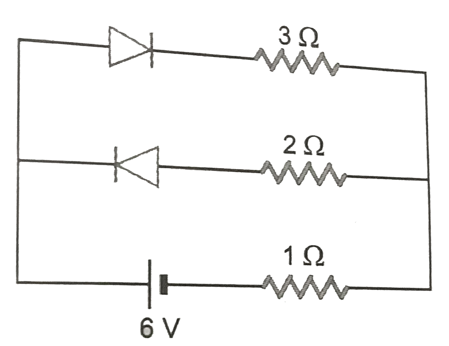
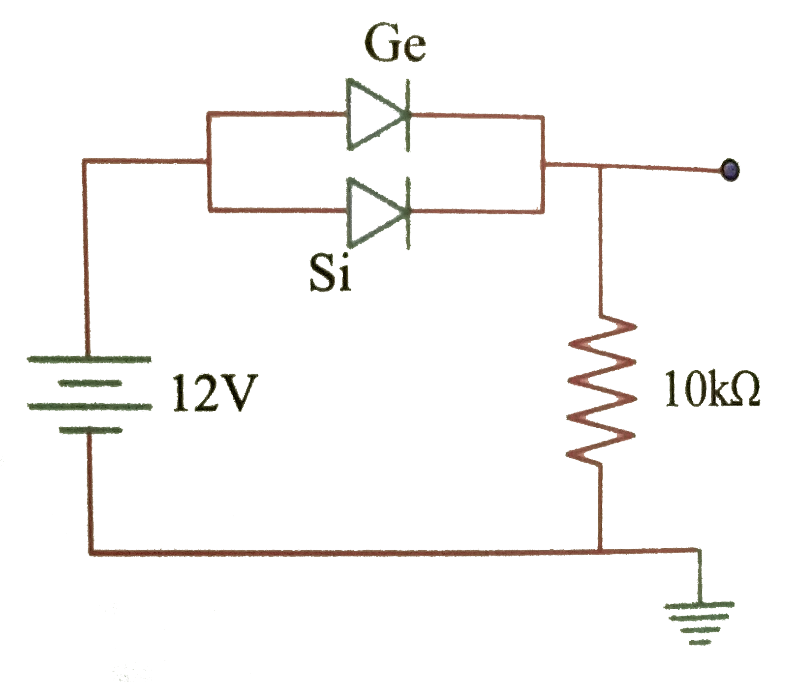
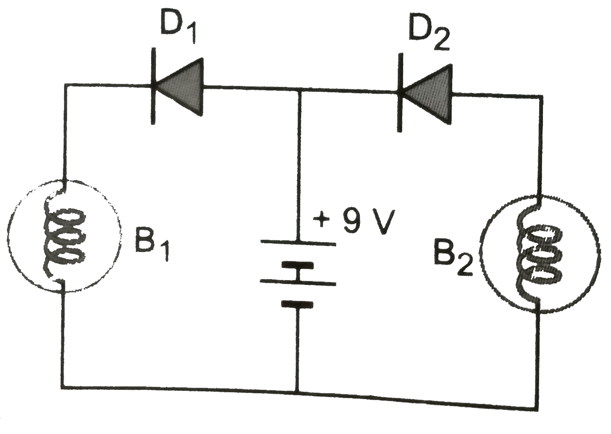
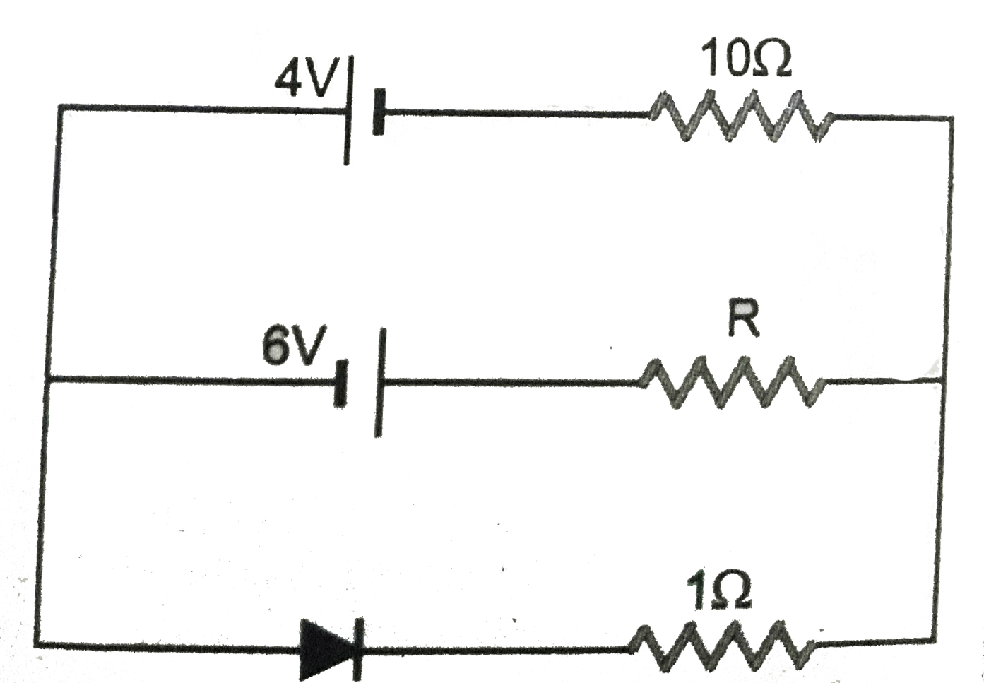
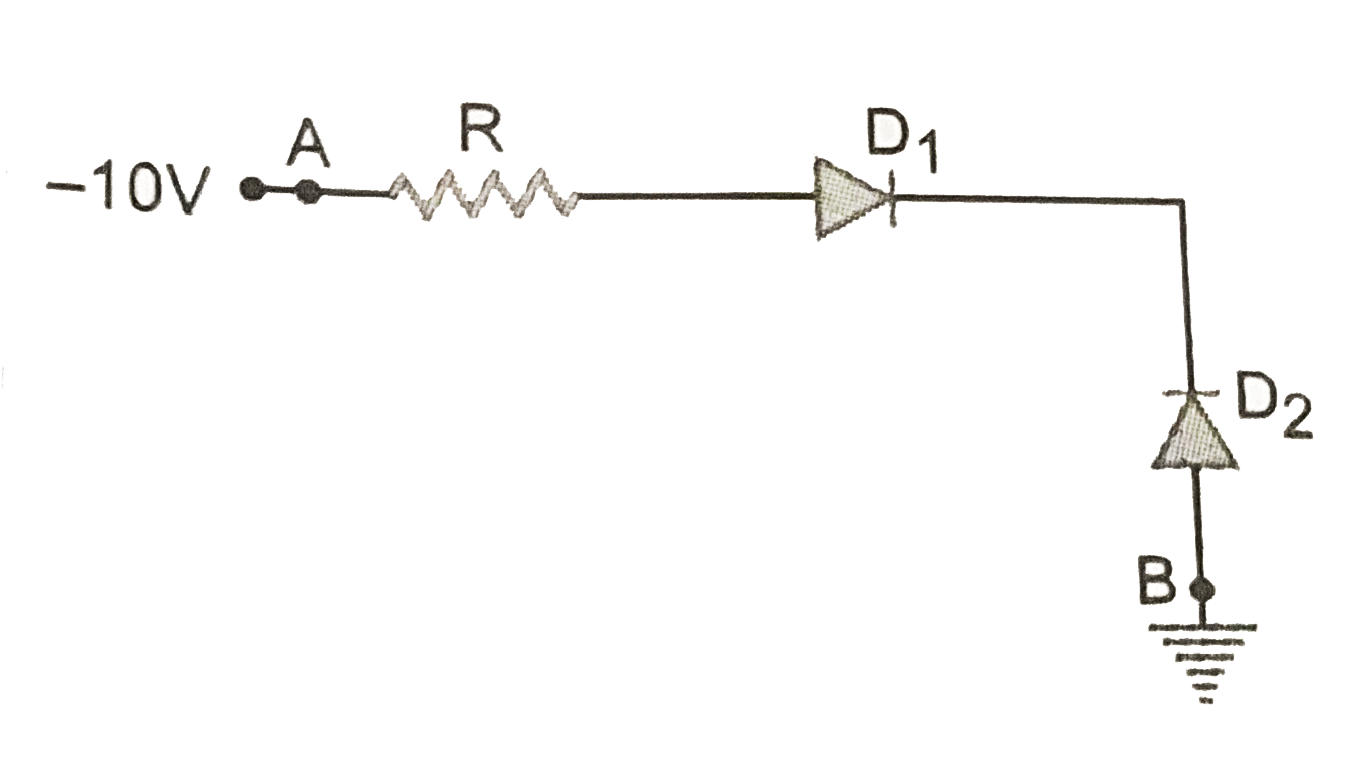
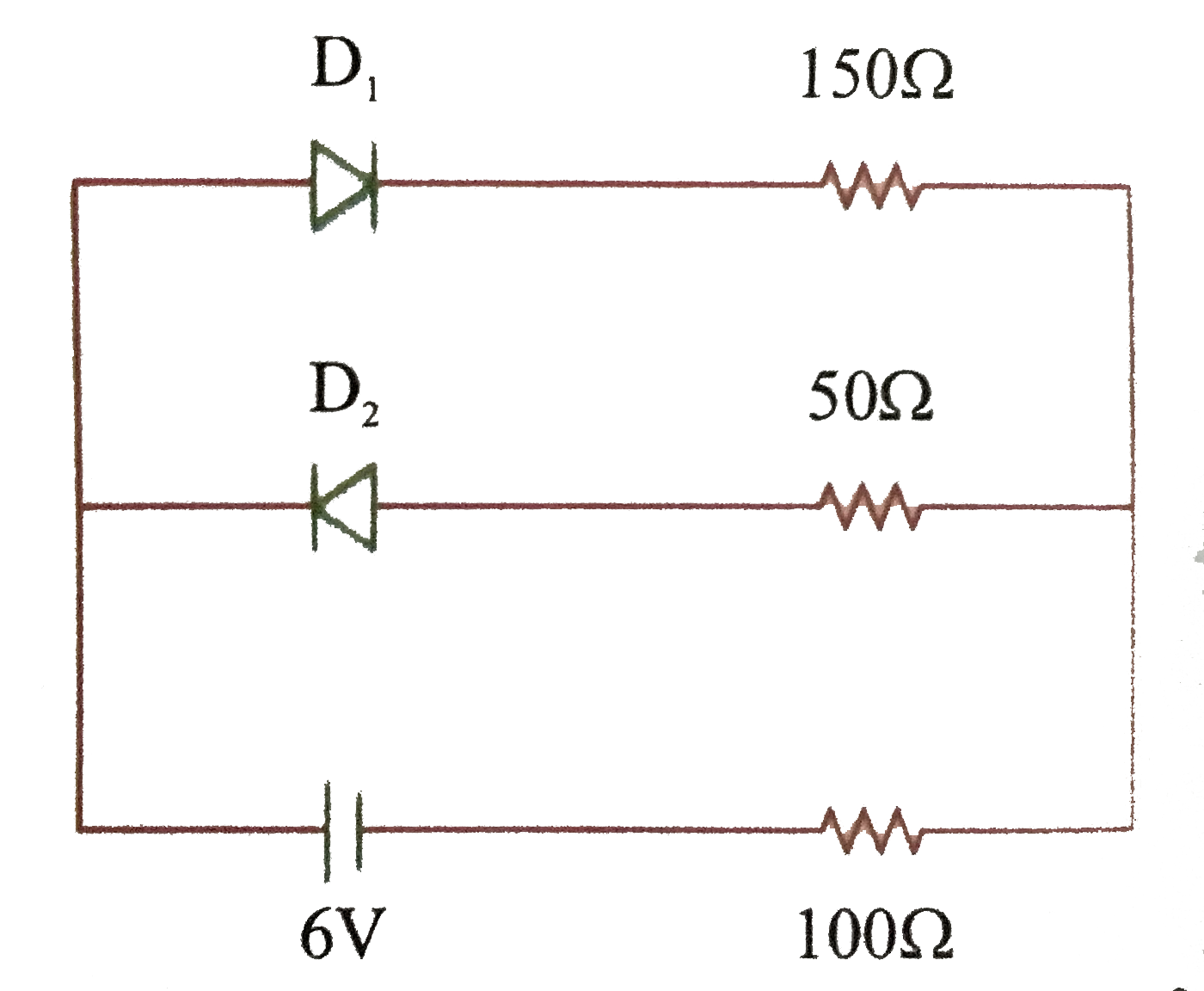
Two junction diodes, one of germanium (Ge) and other of silicon (Si) are connected as shown in fig to a battery of 12V and a load resistance 10kΩ. The germanium diode conducts at 0.3V and silicon diode at 0.7V. When current flows in the circuit, the potential of terminal Y will be
 .View Solution
Question 166
The currect voltage relation of a diode is given by 1=(evanv/T−1)mA where the applied volied V is in volts and the tempetature T is in degree kelvin if a student make an error meassurting ±01V while measuring the current of 5mAat300K what be the error in the value of current in mA View SolutionQuestion 171
A transistor is used in common emitter mode as an amplifier. Then
(1) the base-emitter junction is forward biased
(2) the base emitter junction is reverse biased
(3) the input signal is connected in series with the voltage applied to the base-emitter junction.
(4) the input signal is connected in series with the voltage applied to the base collector junction.View SolutionQuestion 183
A npn transistor is connected in common emitter configuration in a given amplifier. A load resistance of 800Ωis connected in the collector circuit and the voltage drop across 0.96 and the input resistance of the circuit is 192Ω, the voltage gain and the power gain of the amplifier will respectively be : View SolutionQuestion 201
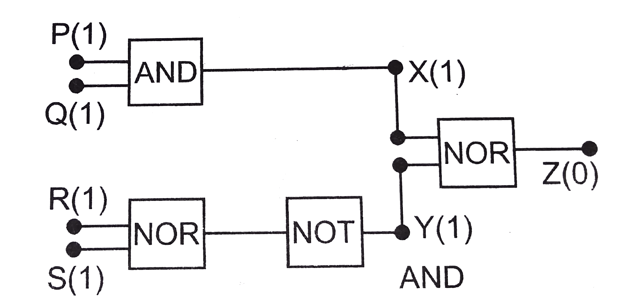
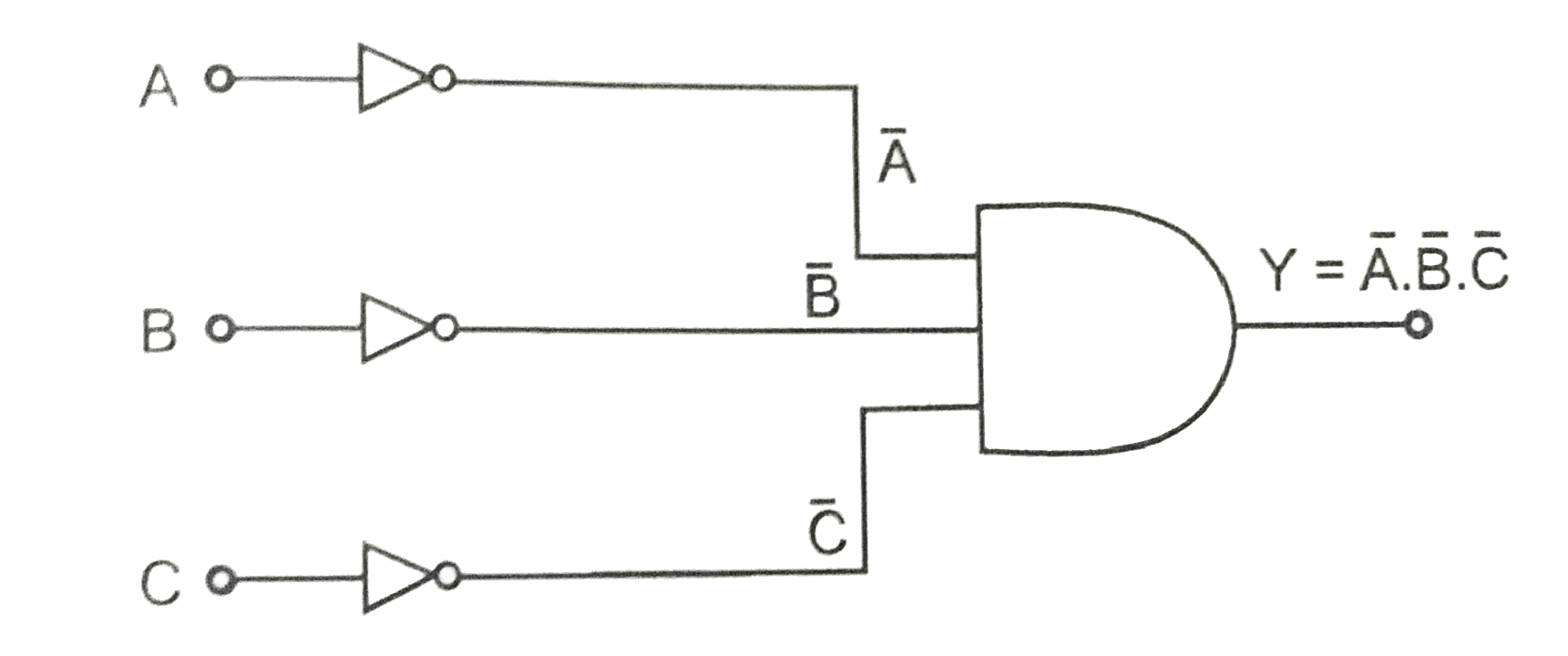
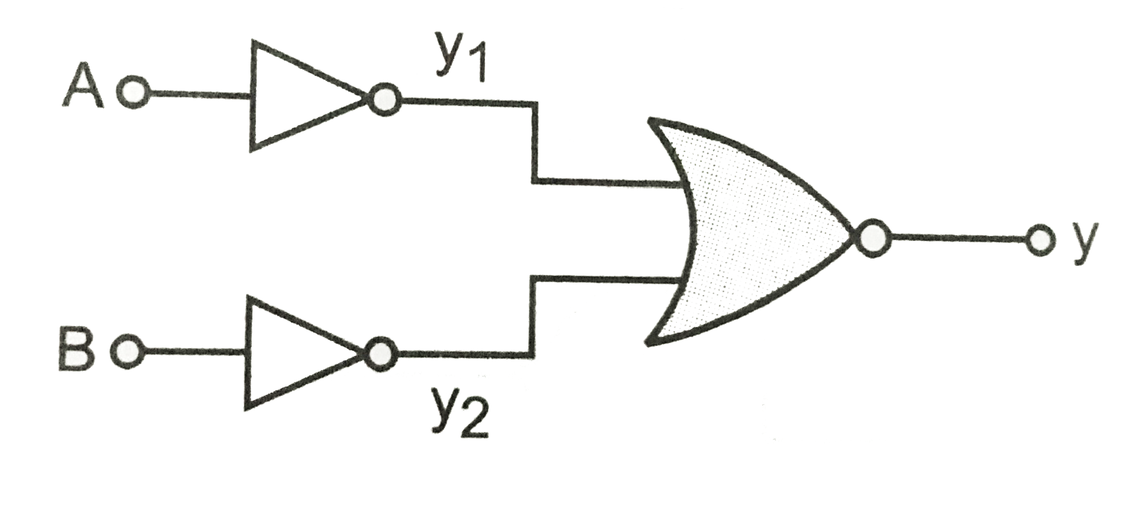
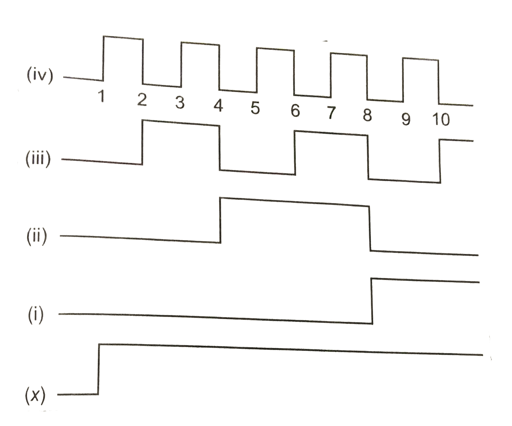
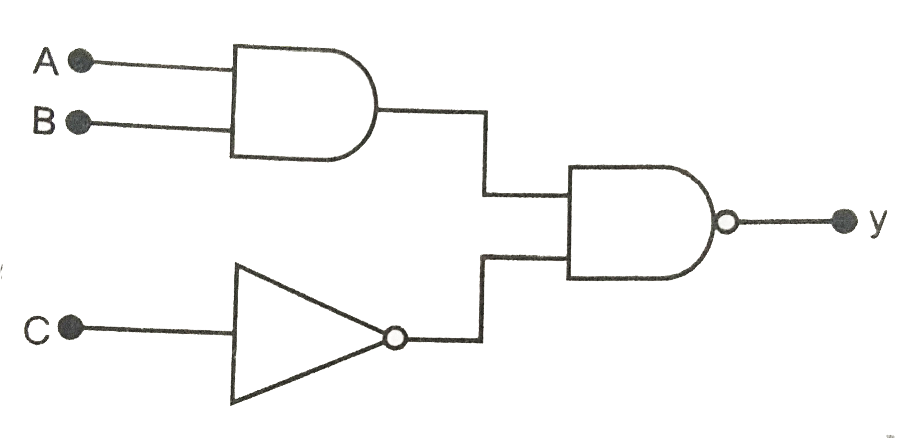
The circuit diagram (see fig.) shows a 'logic combination' with the states outputs X,Y and Z given for input P,Q,R and S all at state 1 (i.e., high). When inputs P and R change to state 0 i.e., low) with inputs Q and S still at 1, the condition of output X,Y and Z chages to
 View Solution
Question 220
A piece of pure semiconductor of silicn of size 1cm×1cm×1mm is having 5×1028 number of atoms per cubic metre. It is doped simultaneously with 5×10²² atoms per m3 of aresenic adn 5×10²⁰ per m3 atoms of indium. The number density of intrisic current carrier (electrons adn holes) in the pure silicon semiconductor is 1.5×10¹⁶m−3. Mobility of electron is 3800cm2V−S−1
The number of electrons in this semiconductor areView SolutionQuestion 221
A piece of pure semiconductor of silicn of size 1cm×1cm×1mm is having 5×1028 number of atoms per cubic metre. It is doped simultaneously with 5×10²² atoms per m3 of aresenic adn 5×10²⁰ per m3 atoms of indium. The number density of intrisic current carrier (electrons adn holes) in the pure silicon semiconductor is 1.5×10¹⁶m−3. Mobility of electron is 3800cm2V−S−1
The number of holes in this semiconductor areView SolutionQuestion 222
A piece of pure semiconductor of silicn of size 1cm×1cm×1mm is having 5×1028 number of atoms per cubic metre. It is doped simultaneously with 5×10²² atoms per m3 of aresenic adn 5×10²⁰ per m3 atoms of indium. The number density of intrisic current carrier (electrons adn holes) in the pure silicon semiconductor is 1.5×10¹⁶m−3. Mobility of electron is 3800cm2V−S−1
The conductivity of doped semiconductor (in Sm−1) isView SolutionQuestion 223
A piece of pure semiconductor of silicn of size 1cm×1cm×1mm is having 5×1028 number of atoms per cubic metre. It is doped simultaneously with 5×10²² atoms per m3 of aresenic adn 5×10²⁰ per m3 atoms of indium. The number density of intrisic current carrier (electrons adn holes) in the pure silicon semiconductor is 1.5×10¹⁶m−3. Mobility of electron is 3800cm2V−S−1
Ratio of conductivity of doped silicon and pure silicon semiconductor is View SolutionQuestion 224
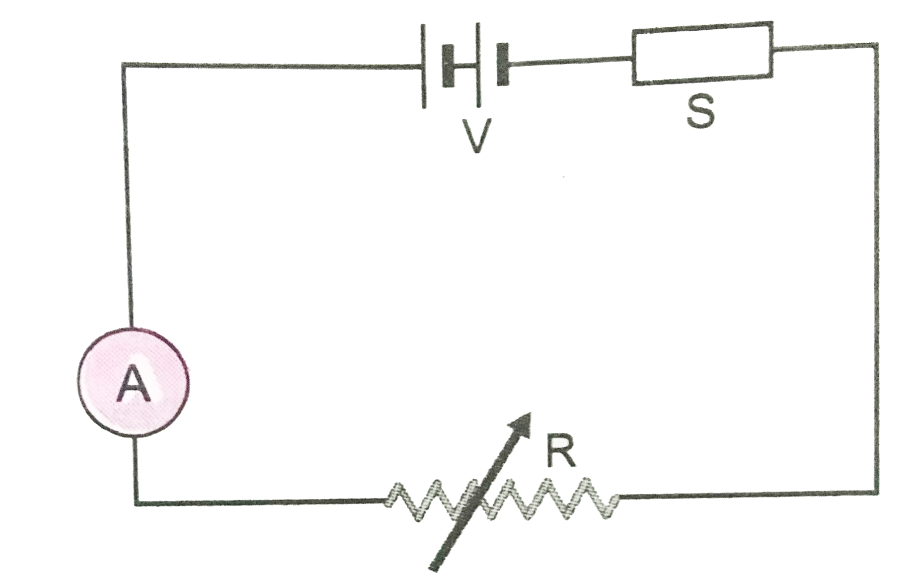
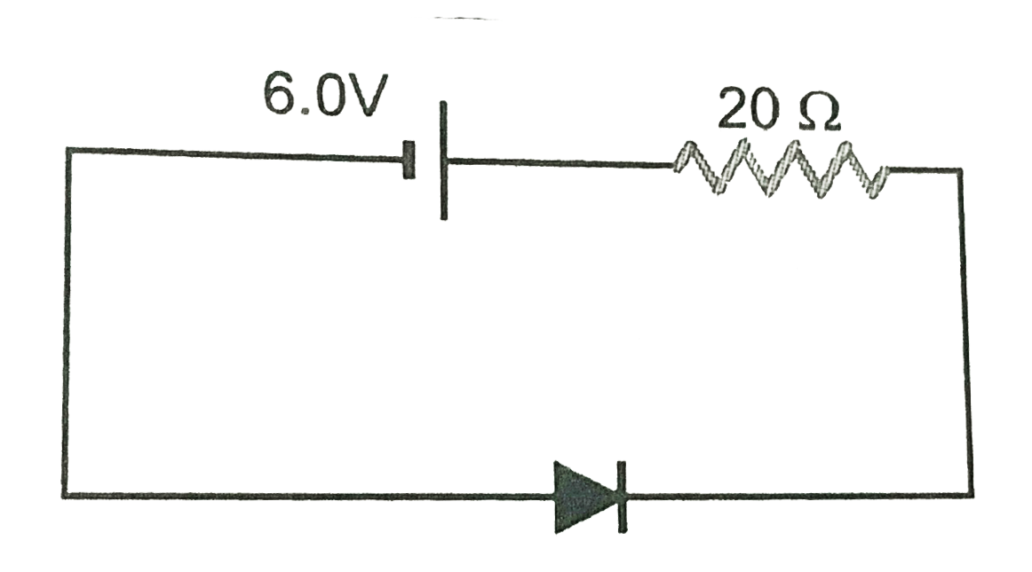
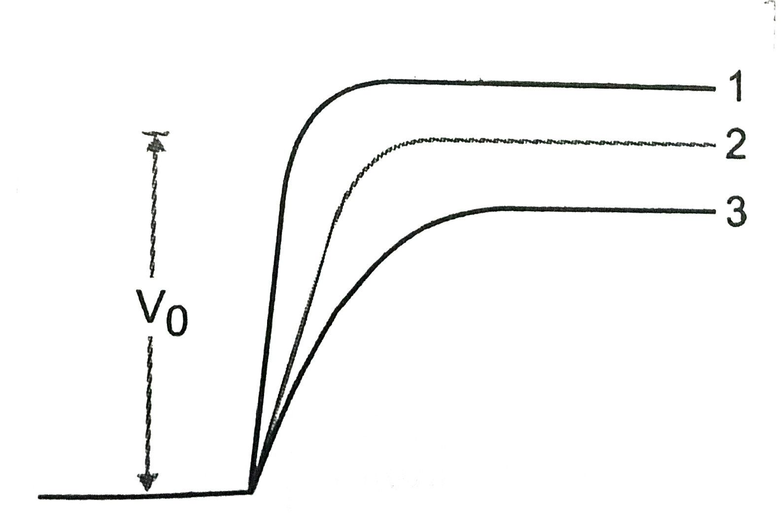
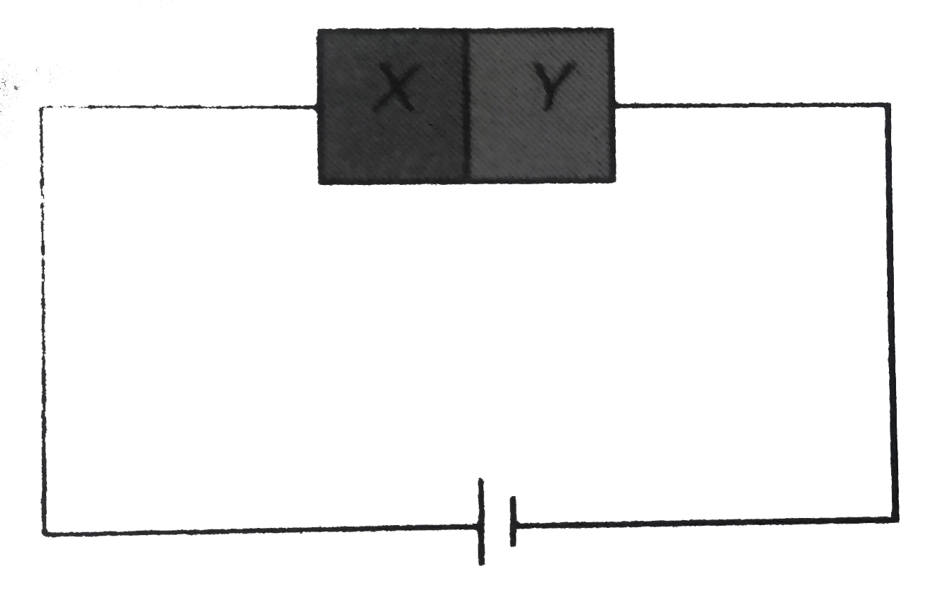
When a p-type semiconductor is brought into a close contact with n-type semiconductor, we get a p-n junction with a barrier potential 0.4V and the width of depletion region is 4.0×10⁻⁷m. this p-n junction is forwaed biased with a battery of voltage 3V adn negligible internal resistance, in series with a resistance of resistance R, ideal milliammeter and key K as shown in Fig.

The intensity of the electric field in the depletion region when p-n junction is unbiased isView SolutionQuestion 225
When a p-type semiconductor is brought into a close contact with n-type semiconductor, we get a p-n junction with a barrier potential 0.4V and the width of depletion region is 4.0×10⁻⁷m. this p-n junction is forwaed biased with a battery of voltage 3V adn negligible internal resistance, in series with a resistance of resistance R, ideal milliammeter and key K as shown in Fig.
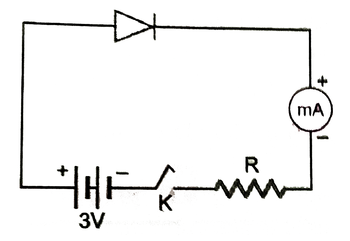
The resistance of resistor R isView SolutionQuestion 226
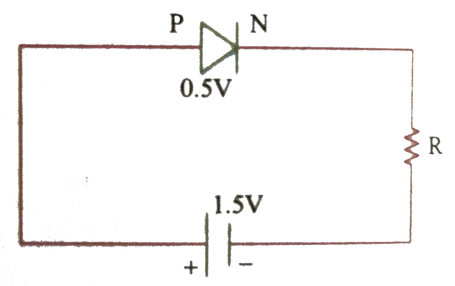
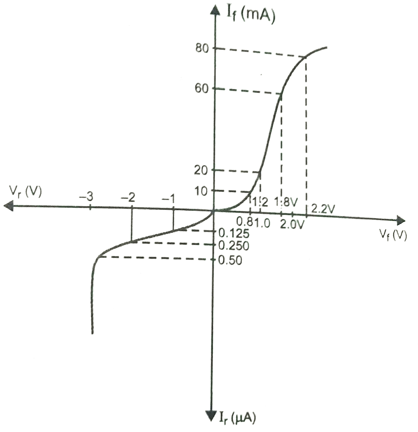
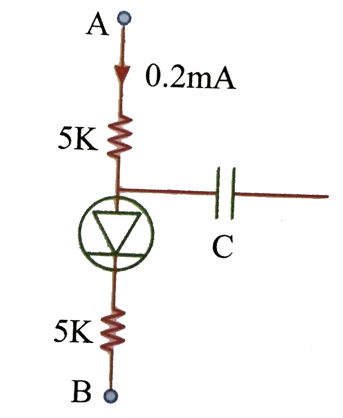
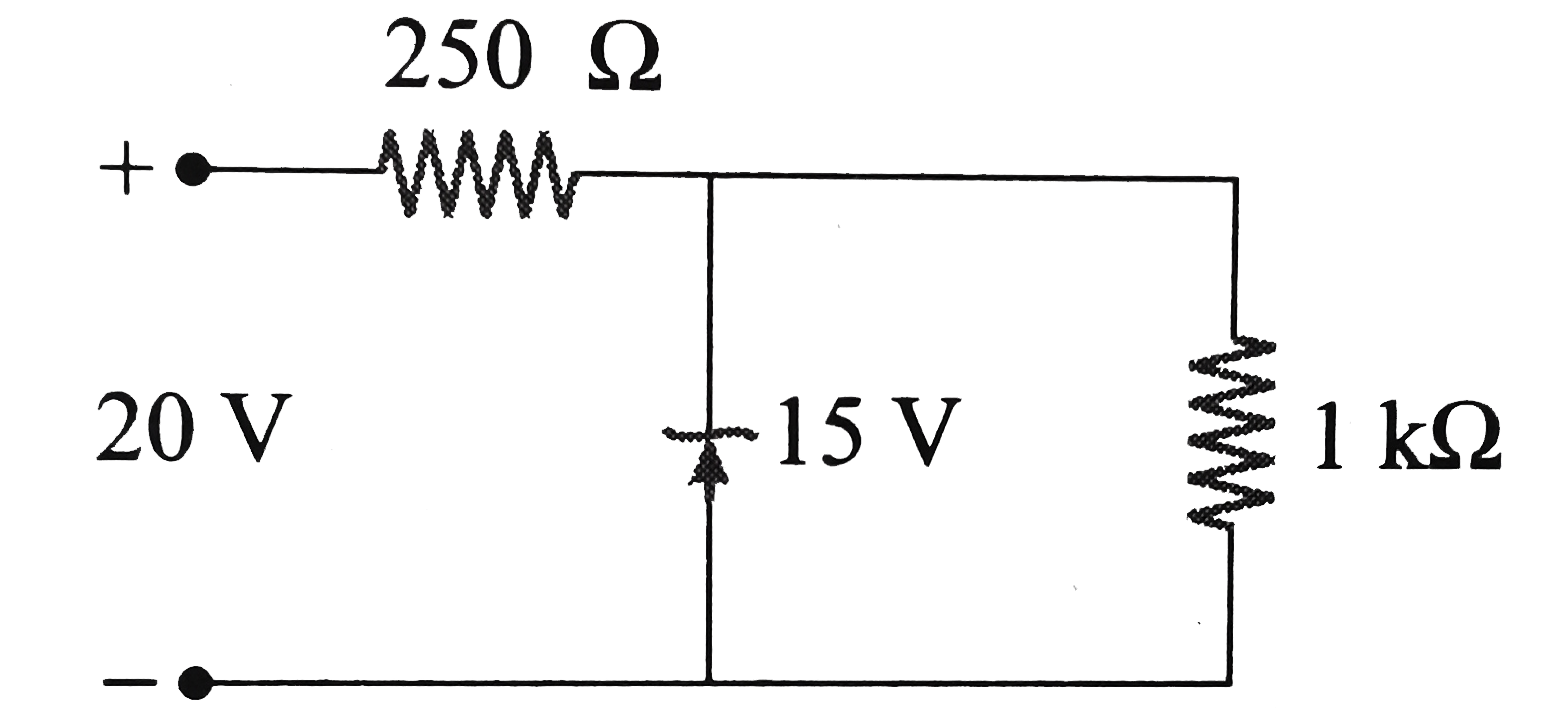
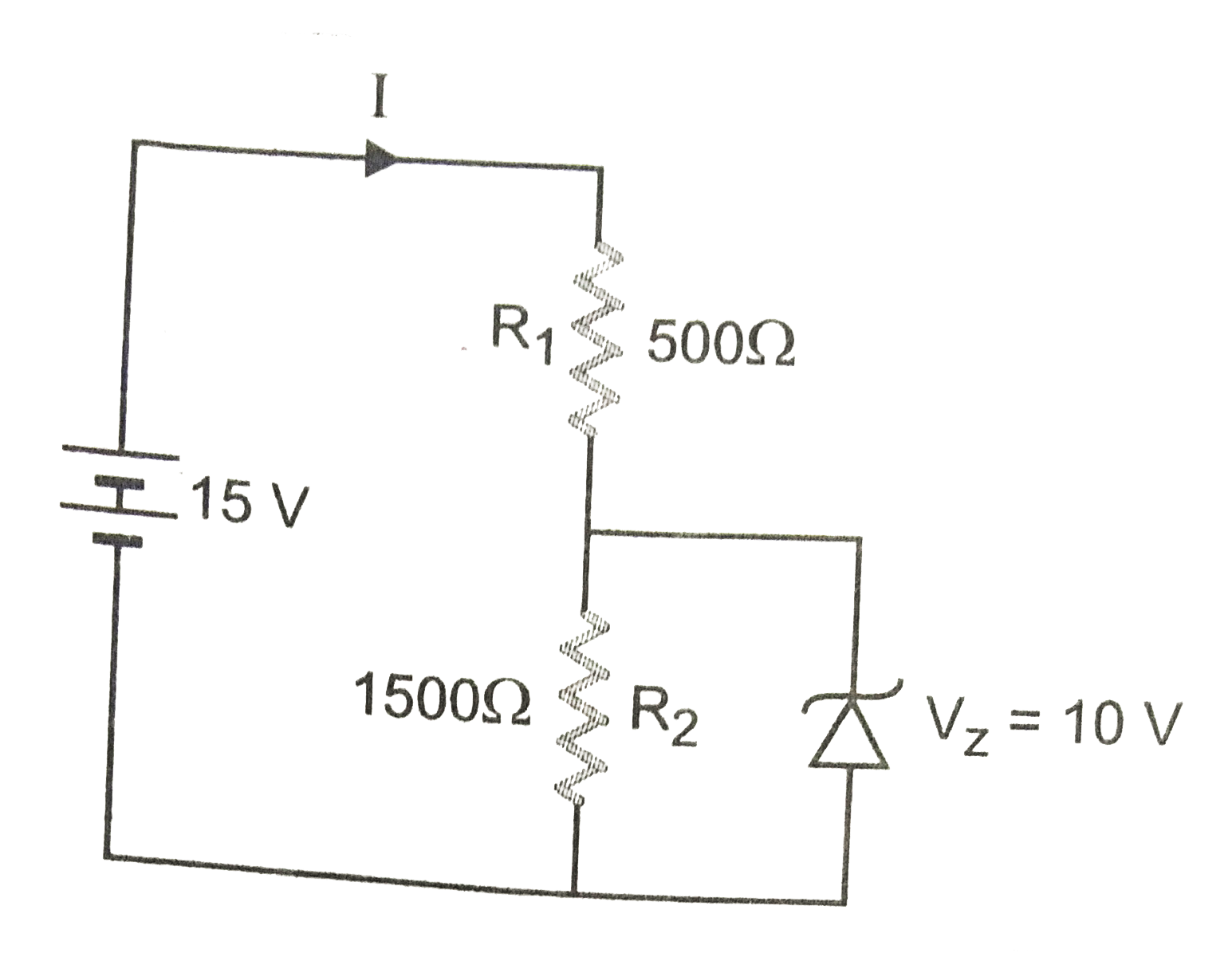
A PN junction diode when forward biased has a drop of 0.5V which is assumed to be independent of current. The current in excess of 10mA through the diode produces large joule heating which damages the diode. If we diode, the resistor used in series with the diode so that the maximum current does not exceed 5mA is.
 .View Solution
Question 230
The number desnity of donor atoms which have to be added to an intrinsic germanium semiconductor to produce an n-type semiconductor of conductivity 5ohm−1cm−1 is a×1015cm−3. Given that the mobility of electron in n-type Ge is 3900cm2/Vs, Neglect the contribution of holes to conductivity. What is the integer value of a?View Solution
All Exercises from PRADEEP PHYSICS Class 12 PHYSICS ELECTRONIC DEVICES
- ADVANCED PROBLEMS FOR COMPETITIONS
- CONCEPTUAL PROBLEMS
- EXERCISES (NCERT)
- Exercise
- Fill in the Blanks
- HIGHER ORDER THINKING SKILLS
- INTEGER TYPE QUESTION
- LONG QUESTION ANSWER
- LONG QUESTION ANSWER (NCERT)
- MCQ
- MULTIPLE CHOICE QUESTIONS
- PROBLEMS FOR PRACTICE
- SAMPLE PROBLEM
- SHORT QUESTION ANSWER
- Solved Examples
- VERY SHORT QUESTION ANSWER (NCERT)

 .
.


 .
.
 .
. .
.
 .
.


 .
.

