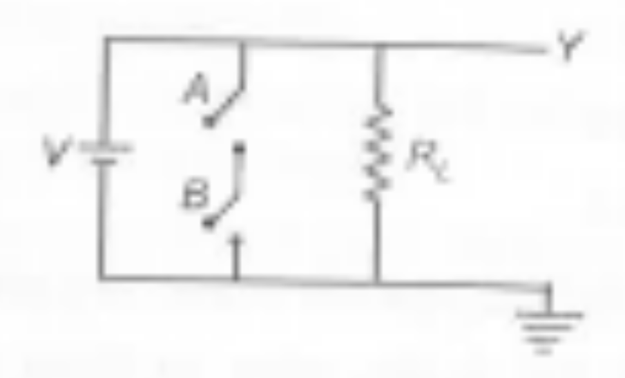
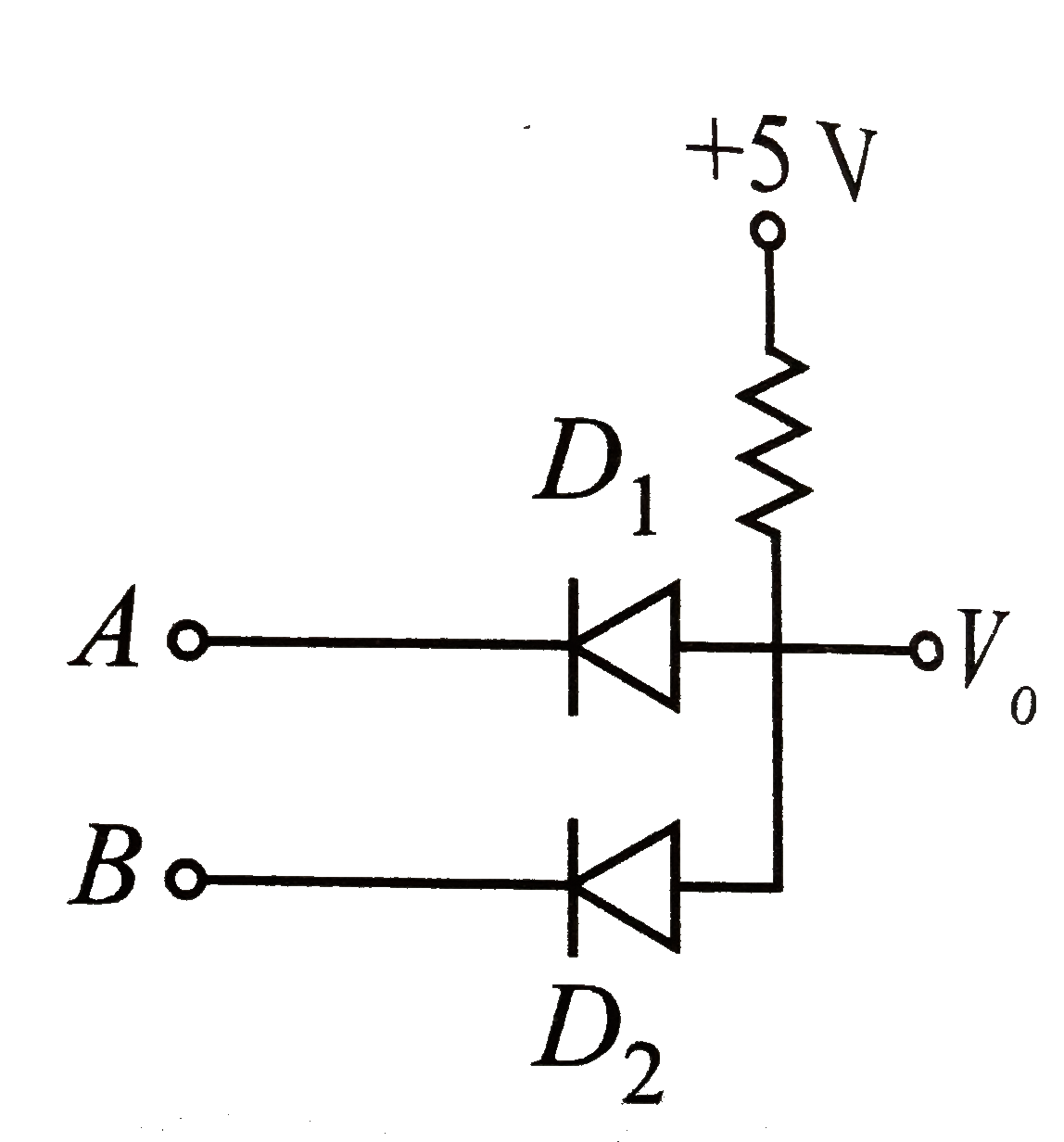
Logic gate realised from pn Junctions shown in figure is
OR gate
AND gate
NOT gate
NOR gate
The correct Answer is:A
To determine the type of logic gate realized from the given PN junctions in the circuit, we will analyze the behavior of the diodes based on the inputs A and B.
1. Identify the Components:
- The circuit consists of two diodes (D1 and D2) connected to points A and B, and the output is taken from point Y, which is connected to a resistor that goes to the ground.
2. Analyze the Input Conditions:
- We will evaluate the output Y for all possible combinations of inputs A and B (0 and 1).
3. Case 1: A = 0, B = 0:
- Both diodes D1 and D2 are reverse-biased (since both inputs are 0).
- Therefore, no current flows, and the output Y = 0.
4. Case 2: A = 0, B = 1:
- D1 is reverse-biased (0V), and D2 is forward-biased (1V).
- D2 conducts, allowing current to flow, hence the output Y = 1.
5. Case 3: A = 1, B = 0:
- D1 is forward-biased (1V), and D2 is reverse-biased (0V).
- D1 conducts, allowing current to flow, hence the output Y = 1.
6. Case 4: A = 1, B = 1:
- Both D1 and D2 are forward-biased.
- Both diodes conduct, allowing current to flow, hence the output Y = 1.
7. Construct the Truth Table:
- Based on the evaluations above, we can summarize the results in a truth table:
| A | B | Output Y |
|---|---|----------|
| 0 | 0 | 0 |
| 0 | 1 | 1 |
| 1 | 0 | 1 |
| 1 | 1 | 1 |
8. Determine the Logic Gate:
- From the truth table, we can see that the output Y is 1 when at least one of the inputs (A or B) is 1. This behavior corresponds to the OR logic gate.
Conclusion:
The logic gate realized from the PN junctions shown in the figure is an OR gate.
- The circuit consists of two diodes (D1 and D2) connected to points A and B, and the output is taken from point Y, which is connected to a resistor that goes to the ground.
- We will evaluate the output Y for all possible combinations of inputs A and B (0 and 1).
- Both diodes D1 and D2 are reverse-biased (since both inputs are 0).
- Therefore, no current flows, and the output Y = 0.
- D1 is reverse-biased (0V), and D2 is forward-biased (1V).
- D2 conducts, allowing current to flow, hence the output Y = 1.
- D1 is forward-biased (1V), and D2 is reverse-biased (0V).
- D1 conducts, allowing current to flow, hence the output Y = 1.
- Both D1 and D2 are forward-biased.
- Both diodes conduct, allowing current to flow, hence the output Y = 1.
- Based on the evaluations above, we can summarize the results in a truth table:
|---|---|----------|
| 0 | 0 | 0 |
| 0 | 1 | 1 |
| 1 | 0 | 1 |
| 1 | 1 | 1 |
- From the truth table, we can see that the output Y is 1 when at least one of the inputs (A or B) is 1. This behavior corresponds to the OR logic gate.
The logic gate realized from the PN junctions shown in the figure is an OR gate.
Topper's Solved these Questions
- SEMICONDUCTOR ELECTRONICS (MATERIAL, DEVICES AND SIMPLE CIRUITS )BOOK - AAKASH INSTITUTE ENGLISHCHAPTER - SEMICONDUCTOR ELECTRONICS (MATERIAL, DEVICES AND SIMPLE CIRUITS )EXERCISE - Assignment section -C (Previous years type question)
110 Videos
- SEMICONDUCTOR ELECTRONICS (MATERIAL, DEVICES AND SIMPLE CIRUITS )BOOK - AAKASH INSTITUTE ENGLISHCHAPTER - SEMICONDUCTOR ELECTRONICS (MATERIAL, DEVICES AND SIMPLE CIRUITS )EXERCISE - Assignment SECTION - D (Assertion & reason type Question)
10 Videos
- SEMICONDUCTOR ELECTRONICS (MATERIAL, DEVICES AND SIMPLE CIRUITS )BOOK - AAKASH INSTITUTE ENGLISHCHAPTER - SEMICONDUCTOR ELECTRONICS (MATERIAL, DEVICES AND SIMPLE CIRUITS )EXERCISE - Assignment section -A (Objective Type Question)
43 Videos
- RAY OPTICS AND OPTICAL INSTRUMENTSBOOK - AAKASH INSTITUTE ENGLISHCHAPTER - RAY OPTICS AND OPTICAL INSTRUMENTSEXERCISE - ASSIGNMENT (SECTION - D)
16 Videos
- SEMICONDUCTOR ELECTRONICS: MATERIALS, DEVICES AND SIMPLE CIRCUITSBOOK - AAKASH INSTITUTE ENGLISHCHAPTER - SEMICONDUCTOR ELECTRONICS: MATERIALS, DEVICES AND SIMPLE CIRCUITSEXERCISE - Assignment (Section-D (Assertion and reason))
5 Videos
Similar Questions
Knowledge Check
Write the truth table for the circuit shown in figure given below. Name the gate that the circuit resembles.
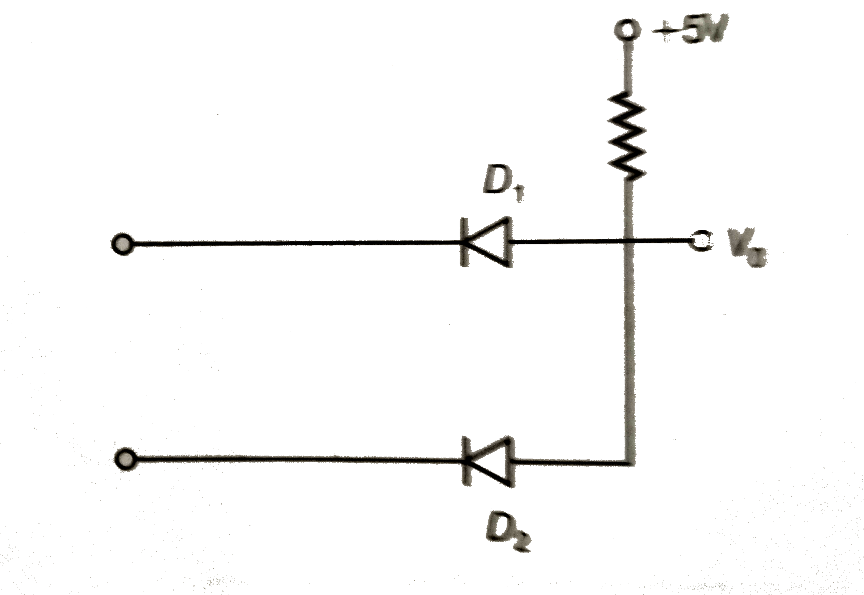 ANANDBANDCORDNOR
The forward characteristic curve of a junction diode is shown in figure below:
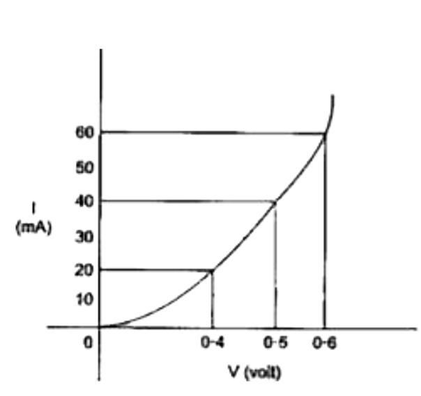
Calculate the resistance of the diode at:
I= 60mA
View SolutionThe forward characteristic curve of a junction diode is shown in figure below:
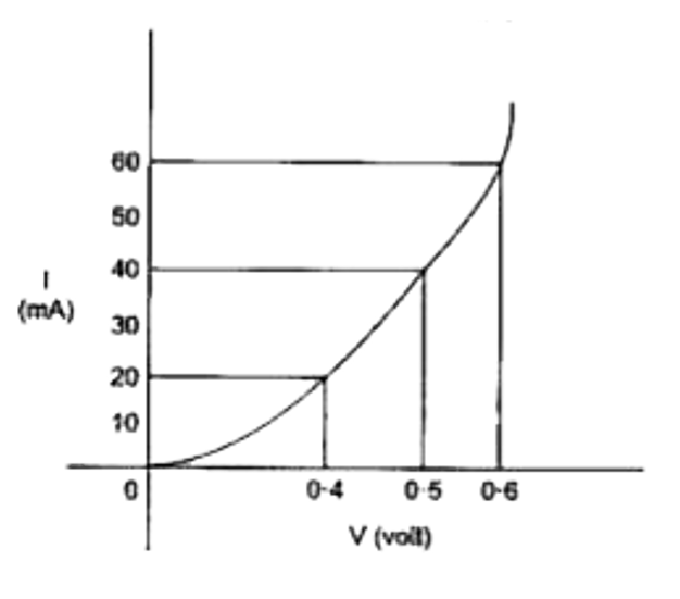
Calculate the resistance of the diode at:
y= 0.5V
View SolutionLogic gate for input A and B is given in figure
_2019_CBT7_E01_022_Q01.png)
Which table is correct for given gates system.
View SolutionStudy the circuits shown in the figure. Name the gate that the given circuit resembles.
View Solution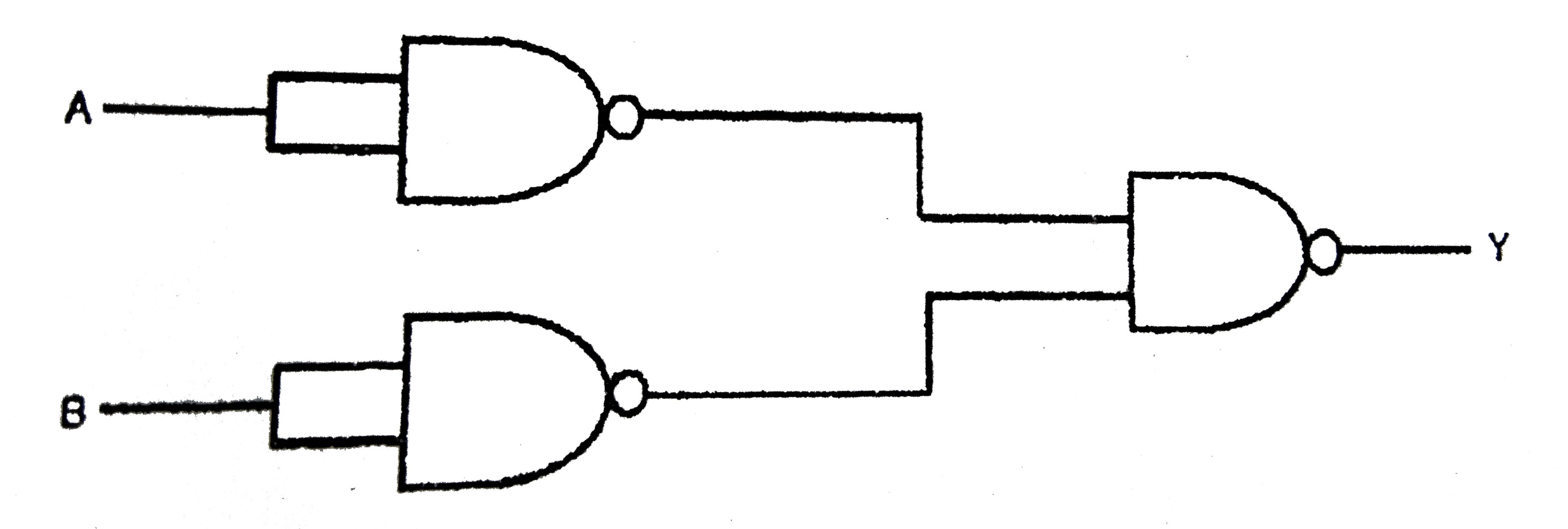
Draw the truth table for the logic gate arrangement shown in the figure.
View SolutionOutput Y of the gate shown in figure
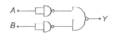
View SolutionPrepare a trith table for the combination of gates shown in figure below:

View Solution

