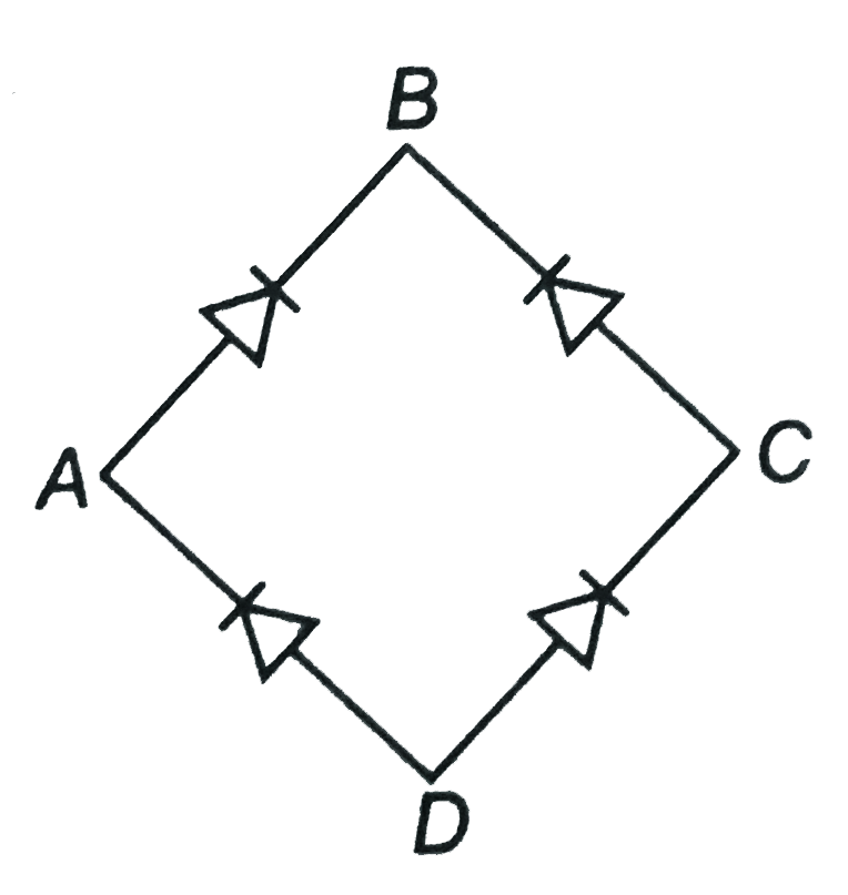
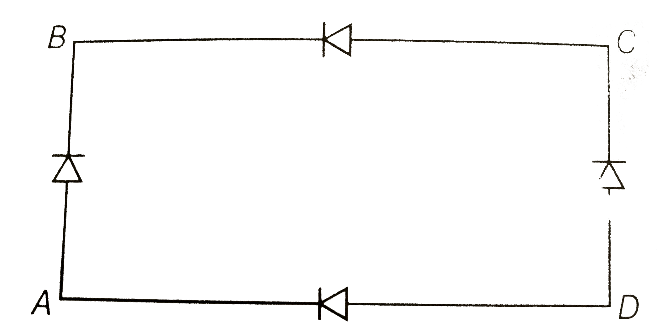
In figure the input is across the terminals A and C and the output is across B and D. Then the output is
Zero
Same as input
Full wave rectified
Half wave rectified
The correct Answer is:C
Step by step video & image solution for In figure the input is across the terminals A and C and the output is across B and D. Then the output is by Physics experts to help you in doubts & scoring excellent marks in Class 12 exams.
Updated on:21/07/2023Topper's Solved these Questions
- SEMICONDUCTOR ELECTRONICS: MATERIALS, DEVICES AND SIMPLE CIRCUITSBOOK - AAKASH INSTITUTE ENGLISHCHAPTER - SEMICONDUCTOR ELECTRONICS: MATERIALS, DEVICES AND SIMPLE CIRCUITSEXERCISE - Assignment (Section -C(Linked comprehension type question))
3 Videos
- SEMICONDUCTOR ELECTRONICS: MATERIALS, DEVICES AND SIMPLE CIRCUITSBOOK - AAKASH INSTITUTE ENGLISHCHAPTER - SEMICONDUCTOR ELECTRONICS: MATERIALS, DEVICES AND SIMPLE CIRCUITSEXERCISE - Assignment (Section-D (Assertion and reason))
5 Videos
- SEMICONDUCTOR ELECTRONICS: MATERIALS, DEVICES AND SIMPLE CIRCUITSBOOK - AAKASH INSTITUTE ENGLISHCHAPTER - SEMICONDUCTOR ELECTRONICS: MATERIALS, DEVICES AND SIMPLE CIRCUITSEXERCISE - Assignment (Section -A (Objective Type question (One option is correct))
50 Videos
- SEMICONDUCTOR ELECTRONICS (MATERIAL, DEVICES AND SIMPLE CIRUITS )BOOK - AAKASH INSTITUTE ENGLISHCHAPTER - SEMICONDUCTOR ELECTRONICS (MATERIAL, DEVICES AND SIMPLE CIRUITS )EXERCISE - Assignment SECTION - D (Assertion & reason type Question)
10 Videos
- SYSTEM OF PARTICLES AND ROTATIONAL MOTIONBOOK - AAKASH INSTITUTE ENGLISHCHAPTER - SYSTEM OF PARTICLES AND ROTATIONAL MOTIONEXERCISE - Try Yourself
63 Videos
Similar Questions
Knowledge Check
The following figure shows a logic gate circuit with two inputs A and B and the output Y. The voltage waveforms of A,B and Y are as given :
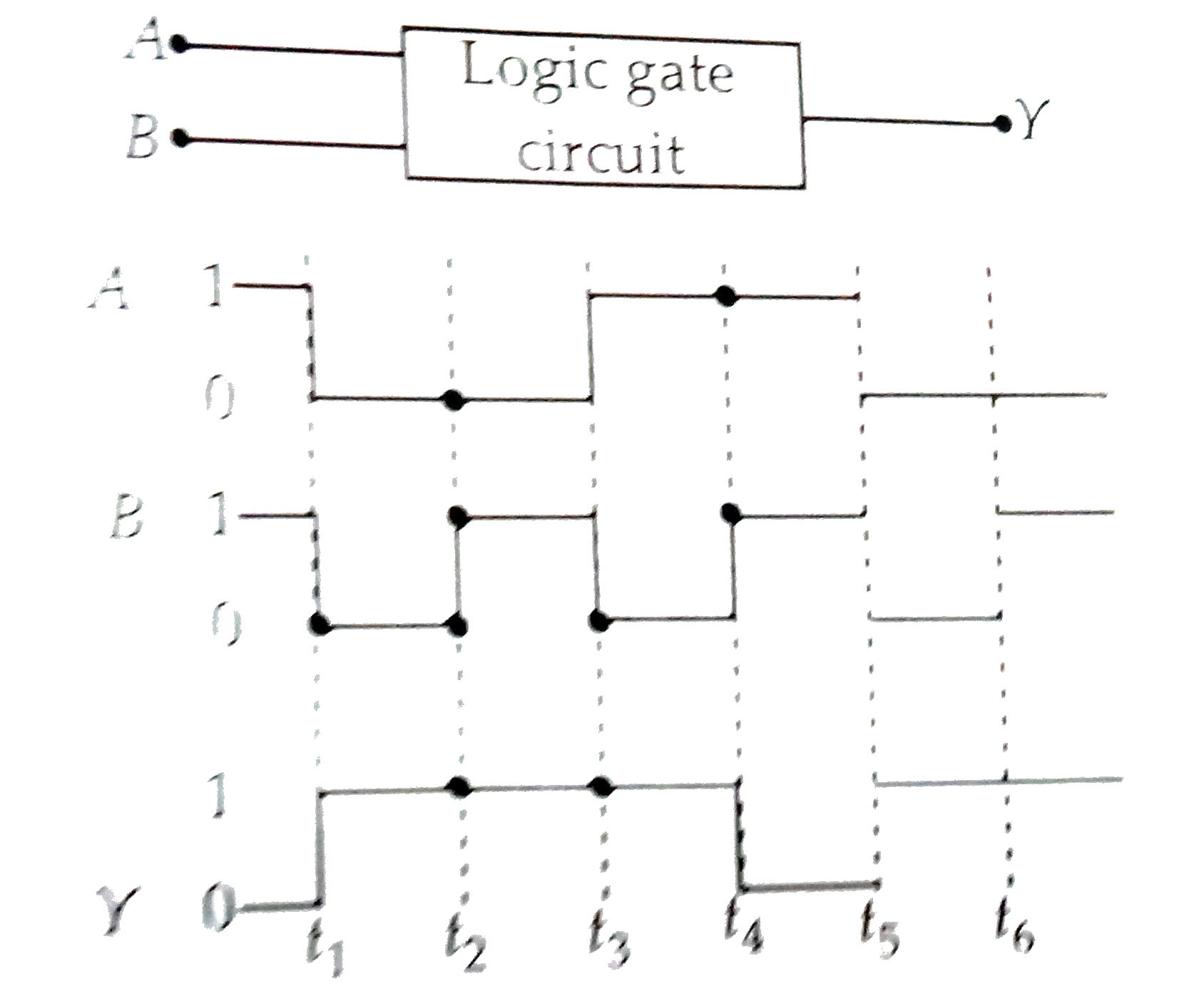
The logic gate isANOR gateBOR gateCAND gateDNAND gate
When the inputs of a two input logic gate are 0 and 0, the output is 1. When the inputs are 1 and 0, the output is zero. The type of logic gate is
View Solution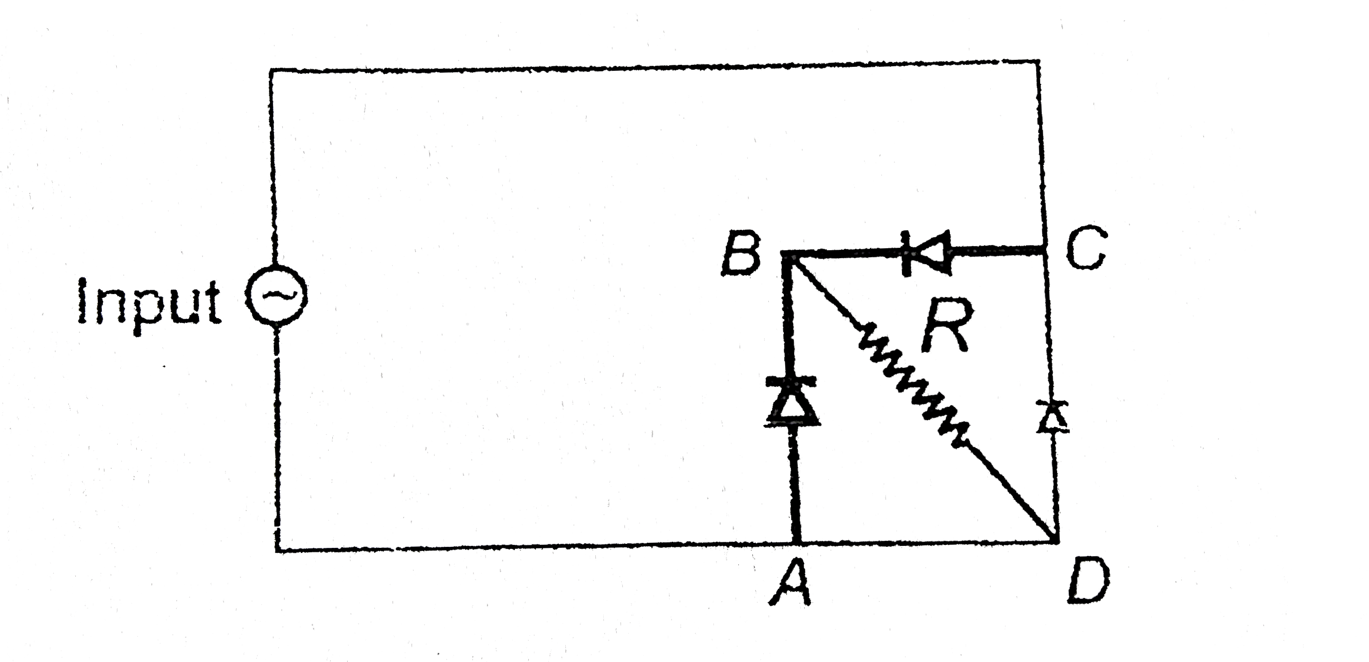
If the input is given between A and C, thent he output at the ends of R will be
View SolutionPotential difference across the terminal of a non ideal battery is
View SolutionThe following figure shows a logic gate circuit with two inputs A and B and the output C. The voltage waveforms of A, B and C are as given The logic circuit is:
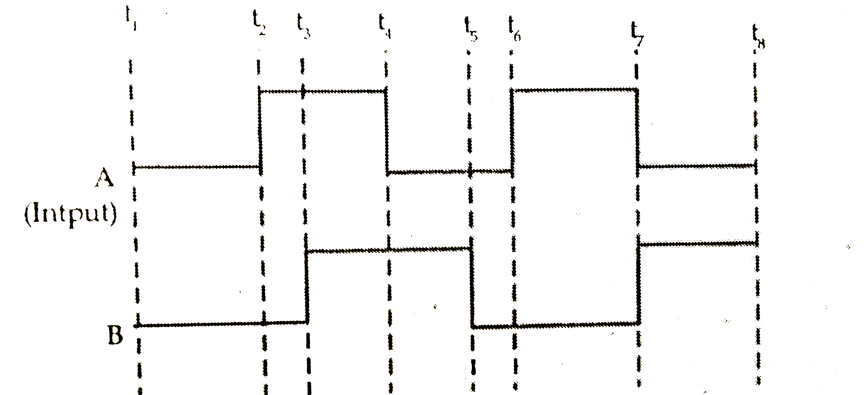
View SolutionThe figure shows the input weveforms A and B for 'AND' gate Draw the output waveform and write the truth table for this logic gate
 .
.
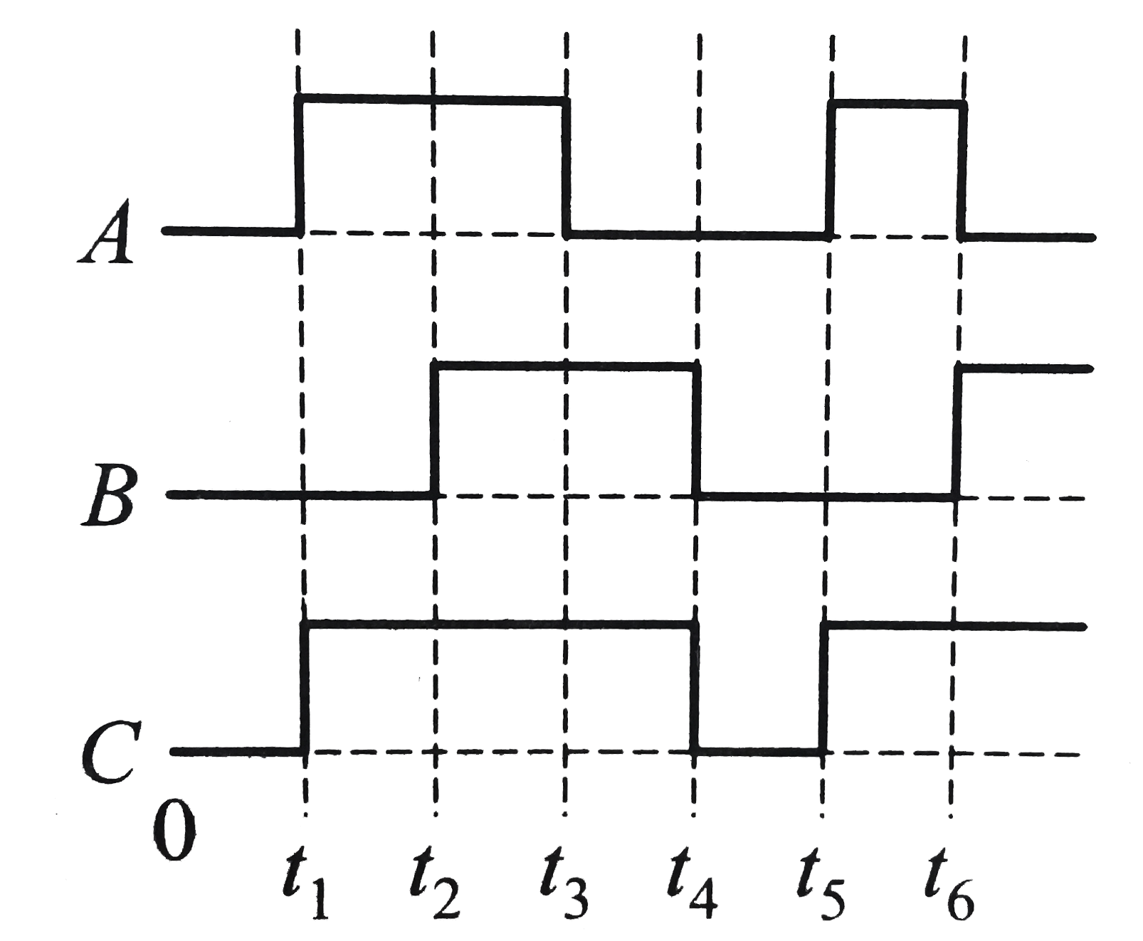
View SolutionThe figure shows a logic circuit with two inputs A and B and the output C. The voltage wave forms across A,B and C are as given. The logic circuit gate is
View SolutionIf A & B are the input as shown in the figure , then output will be

View Solution

