For the given input voltage wavelength Vin(t) , the output voltage waveform (V0)(t) , across the capacitor is correctly depicted by :
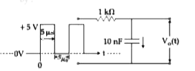
Option1 
Option2 
Option3 
Option4 
Step by step video & image solution for For the given input voltage wavelength V_("in")(t) , the output voltage waveform (V_0)(t) , across the capacitor is correctly depicted by : by Physics experts to help you in doubts & scoring excellent marks in Class 12 exams.
Updated on:21/07/2023Topper's Solved these Questions
Similar Questions
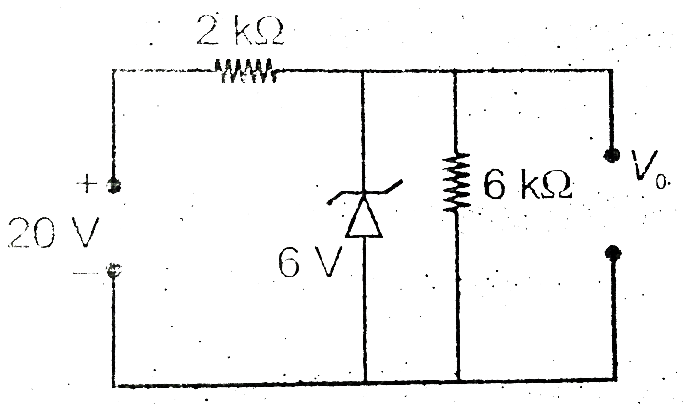
What is the value of output voltage V0 in the circuit shown in the figure ?
View SolutionAssertion (A):∧m(H⊕) and ∧m(cOH) ions are very much higher than those of other ions.
Reason (R):It is due to proton jump from one water molecule to another resulting in a more rapid transfer of positive charge form one region to another.
(a)If both (A) and (R) are correct, and (R) is the correct explanation of (A).
(b)If both (A) and (R) are correct, but (R) is not the correct explanation of (A).
(c)If (A) is correct, but (R) is incorrect.
(d)If (A) is incorrect, (R) is correct.
View Solution
Knowledge Check
The following figure shows a logic gate circuit with two inputs A and B and the output Y. The voltage waveforms of A,B and Y are as given :
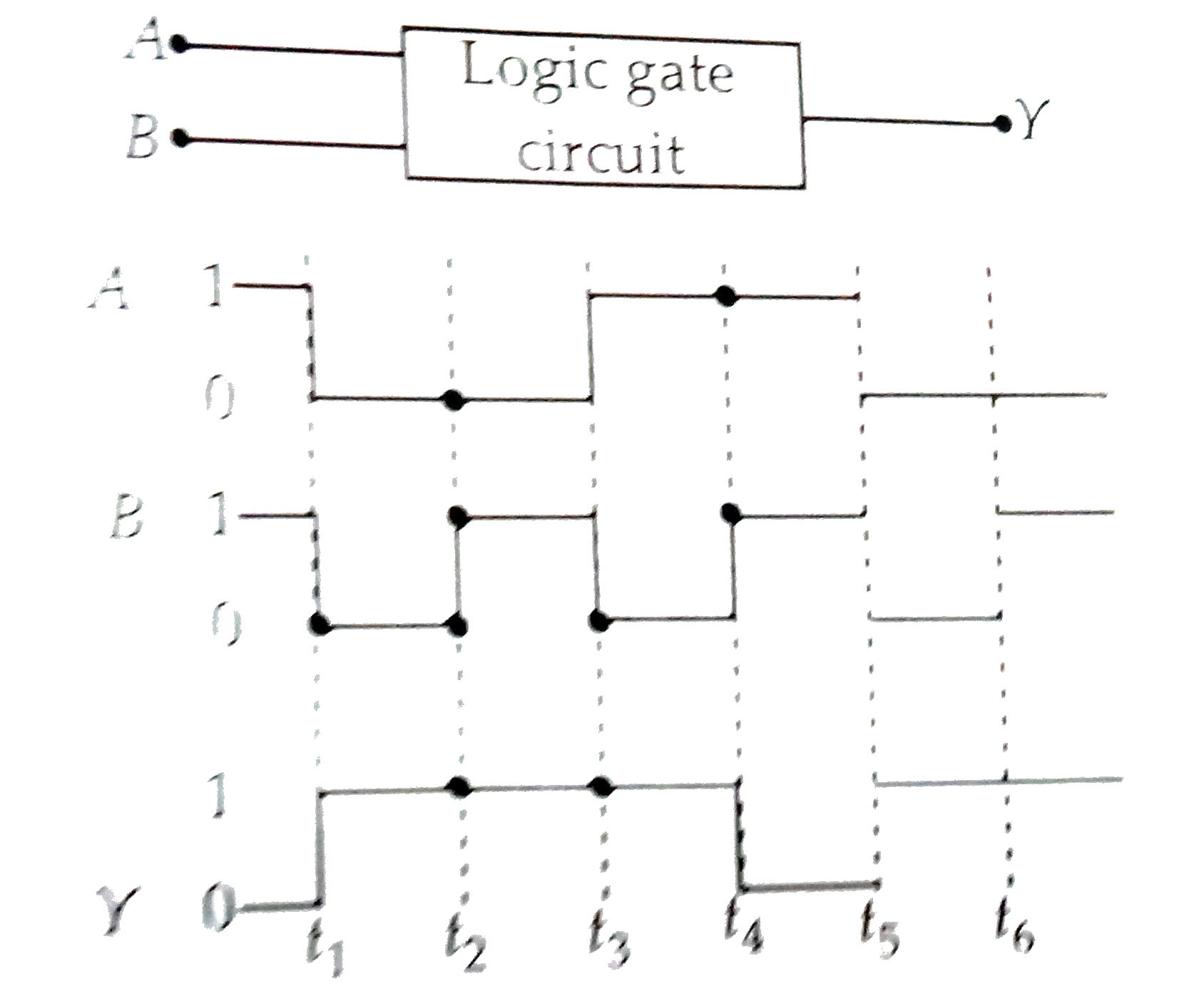
The logic gate isANOR gateBOR gateCAND gateDNAND gate
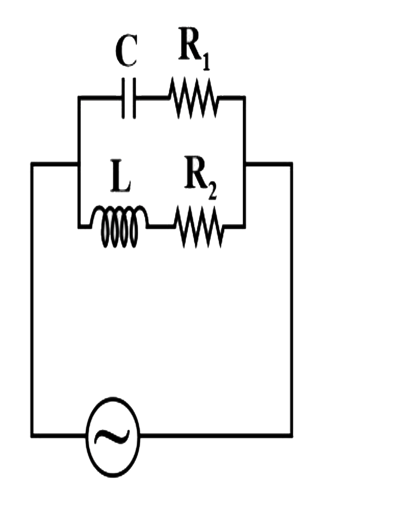
In the given circuit the R.M.S values of voltages across the capacitor C, inductor L and resistor R1 are 12V, 10V and 5 V respectively. Then the peak voltage across R2 is
View SolutionTake the breakdown voltage of the zener diode used in the given circuit as 6V. For the input voltage shown in figure below , the time variation of the output voltage is : (Graphs drawn are schematic and not to scale )

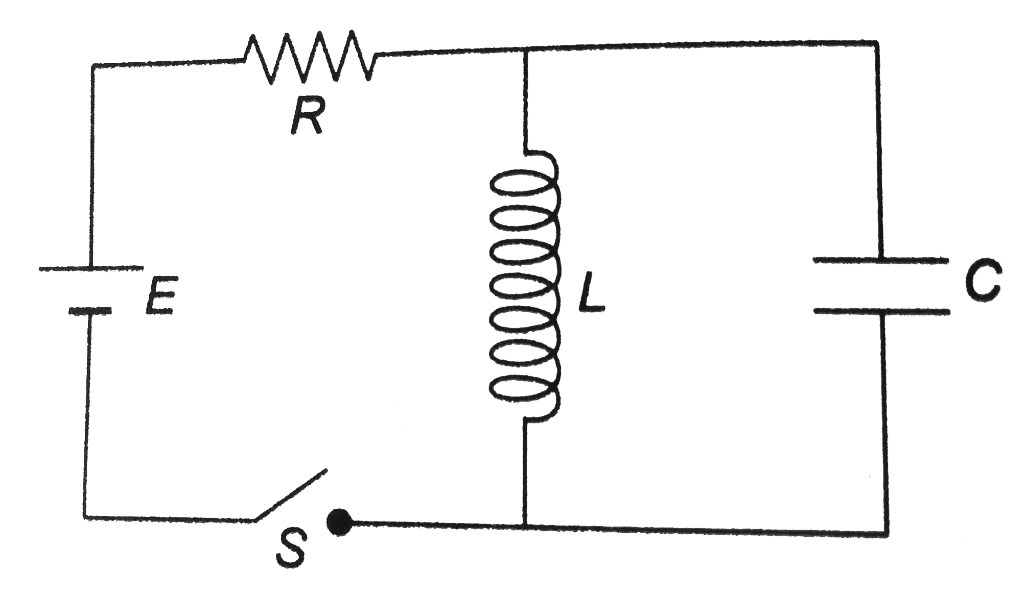
View SolutionIn the circuit shown in the figure, E=50.0V,R=250Ω and C=0.500μF. The switch S is closed for a long time, and no voltage is measured across the capacitor. After the switch is opened, the voltage across the capacitor reaches a maximum value of 150V. What is the inductance L?
View SolutionIf the current through an inductor of 2 H is given by I=tsintA, then the voltage across the inductor is
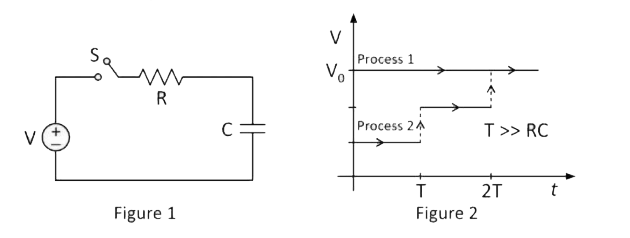
View SolutionProcess 1 : In the circuit the switch S is closed at and the capacitor is fully charged to voltage v0 (i.e., charging continues for time T >> RC). In the process some dissipation (ED) occurs across the resistance R. The amount of energy finally stored in the fully charged capacitor is EC.
Process 2 : In a different process the voltage is first set to v03 maintained for a charging time T >> RC. Then the voltage is raised to 2V03 without discharging the capacitor and again maintained for a time T >> RC. The process is repeated one more time by raising the voltage to v0 and the capacitor is charged to the same final voltage v0 as in process 1. These two processes are depicted in Figure 2.
In Process 2, total energy dissipated across the resistance ED is :
View SolutionThe following figure shows a logic gate circuit with two inputs A and B and the output C. The voltage waveforms of A, B and C are as given The logic circuit is:
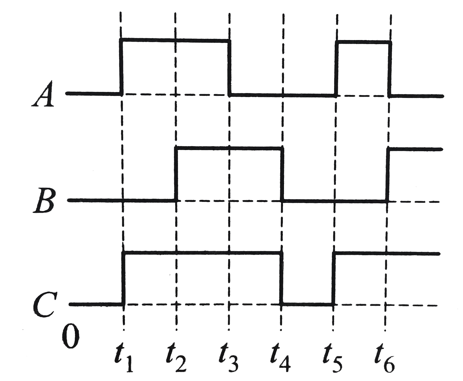
View SolutionThe figure shows a logic circuit with two inputs A and B and the output C. The voltage wave forms across A,B and C are as given. The logic circuit gate is
View Solution
